
XJTAG Layout Viewer
XJTAG Layout Viewer is a free, easy-to-use tool for viewing and inspecting PCB layouts using design data in ODB++ format, which can be exported from any of the major Electronic Design Automation (EDA) tools. It provides a clear and intuitive way to explore board layouts, helping you quickly locate devices, pins and nets and understand board structure without the complexity of full CAD environments.
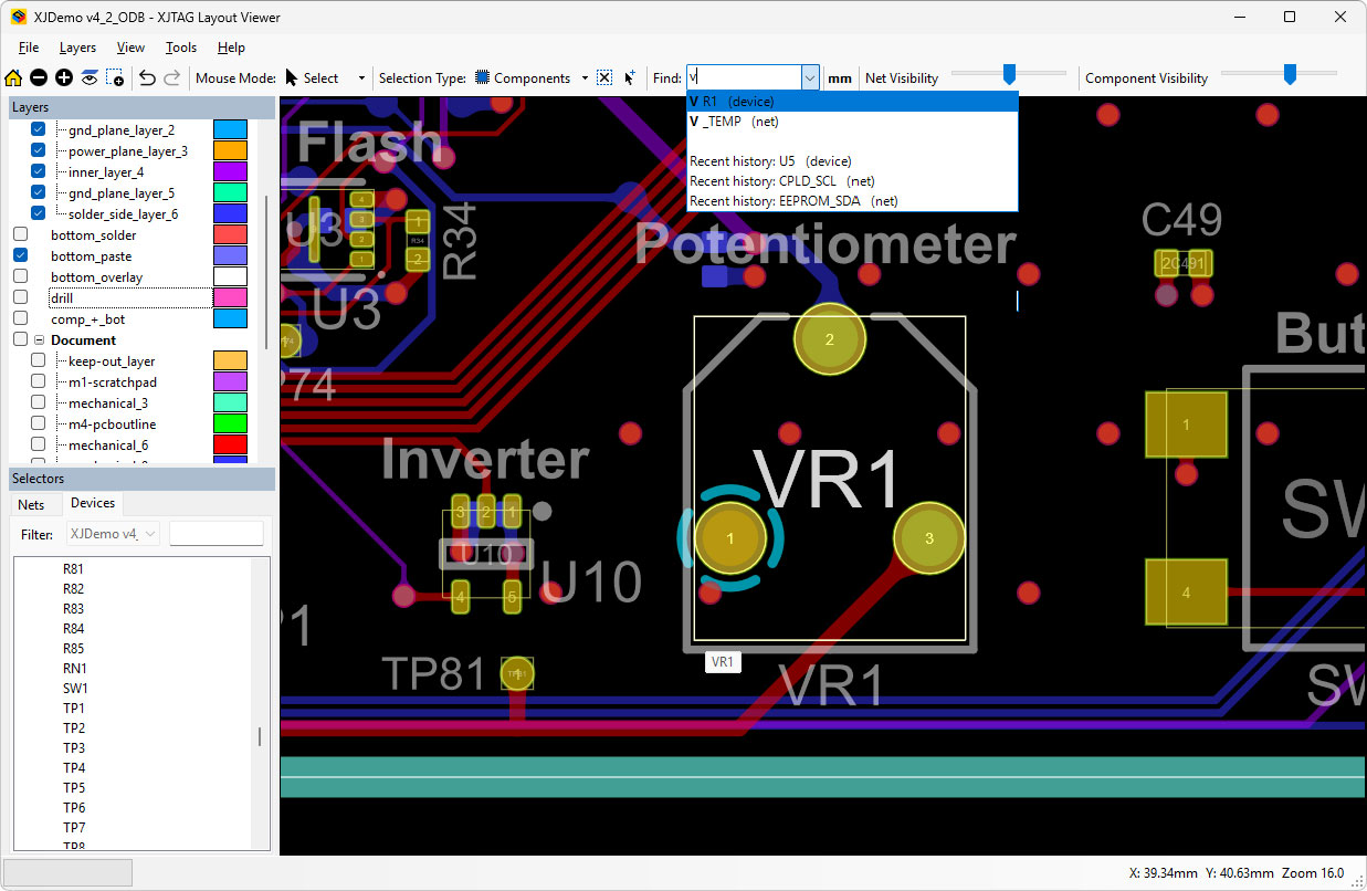
With fast search and net-based highlighting, the viewer makes it easy to navigate complex designs and identify exactly where signals and components are located on the PCB.
Key benefits
Free-of-charge
Free ODB++ PCB viewer for layout exploration, from design to manufacturing data
Clear Connectivity
Understand connections at a glance with net highlighting
Optimised for Speed
Fast loading offline desktop application with high-performance graphics
Easy to use
Quickly locate components, pins and nets on complex PCBs
Improved Productivity
Work more efficiently during inspection, debugging and repair
Lightweight Setup
Easy to install and run with minimal setup required
Visualise Circuit Elements
Selected components and nets are clearly highlighted within the graphical display, making it easy to follow connections and understand circuit structure. Individual layers can be turned on or off to focus on specific areas of the design.
Navigate by Nets
Select or search for nets, components or pins and instantly highlight them on the layout. Combined with zoom, pan and layer controls, this enables fast and efficient exploration of even complex PCB designs.
Clear Inspection and Communication
Inspect individual layout features such as pads, vias, and traces, and view associated information directly within the tool. Export an image of the current view to support design reviews, manufacturing discussions, and issue tracking.
Features
- Search for and highlight components, pins and nets
- Net-based navigation across the PCB layout
- Launch from the command line and jump to specific nets, devices, or pins
- Pan, zoom, rotate and search the layout, including viewing the underside of the board
- Clear visualisation of connections and board structure
- Show or hide individual layers
- Customise layer colours
- Measurement of distances between objects
- Navigate selection history
- Fast loading of ODB++ manufacturing data
- Lightweight desktop tool with no licensing requirements
- Export image of current view to file or printer
- GPU accelerated rendering
- Comprehensive web based help
Documentation
Online Help for XJTAG Layout Viewer is available at any time. You can access this via the Help menu within the application.
Recommended system requirements
- Intel® Core i3, i5, i7 processor or equivalent (any generation)
- Microsoft® Windows® 11
- 8 GB of RAM
XJBoardExplorer allows you to open the board schematic and BOM information, with links going directly to and from the Layout Viewer.
Find a net on one and immediately display it in the other.
Explore XJBoardExplorerXJTAG Layout Viewer is available for quick reference as you configure boundary scan testing on your board in XJDeveloper.
XJRunner and XJInvestigator can use Layout Viewer to display the locations of faults.
Explore XJTAG Test Suite