What is JTAG and how can I make use of it?
JTAG refers to the boundary scan architecture standardised as IEEE 1149.1, defining the Test Access Port (TAP) and associated registers for standardized test access to integrated circuits and circuit board assemblies. Developed to enable structural PCB testing without physical probing of every signal, it improves test coverage and fault isolation.
Although widely used for embedded debug and in-system programming (ISP), these applications build upon the underlying boundary scan infrastructure originally intended for manufacturing test.
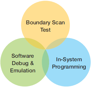
You may be familiar with JTAG because you have used tools with a JTAG interface. Processors often use JTAG to provide access to their debug/emulation functions and all FPGAs and CPLDs use JTAG to provide access to their programming functions.
JTAG is not JUST a technology for processor debug/emulation.
JTAG is not JUST a technology for programming FPGAs/CPLDs.
The debug and programming tools commonly associated with JTAG only make use of one aspect of the underlying technology – the four-wire JTAG communications protocol. Collectively known as the Test Access Port (or TAP), the four standard JTAG TAP pins are: TCK (Test Clock), TMS (Test Mode Select), TDI (Test Data In), TDO (Test Data Out) plus the optional TRST* (Test Reset). These signals control a TAP state machine and allow devices to be connected in a JTAG scan chain.
JTAG pin layout:
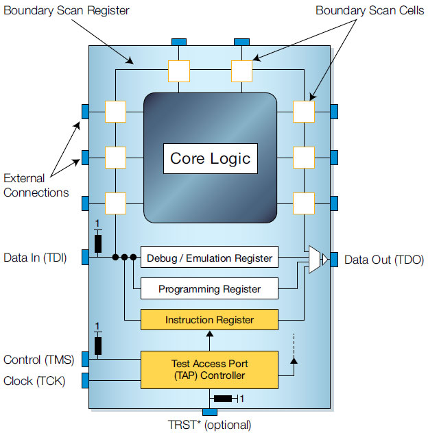
These four signals are part of IEEE Std. 1149.1. This standard was developed to provide a technology for testing Printed Circuit Board Assemblies (PCBAs) without needing the level of physical access required for bed-of-nails testing or the amount of custom development needed for functional test. The TAP was designed to interact with new registers that were added to devices to implement this method of testing.
Very quickly however silicon manufacturers recognised the benefits of using the TAP to access registers offering other functionalities such as debug and programming.
The main register added to a device specifically for JTAG testing is called the Boundary Scan Register (BSR). As its name suggests the individual bits, or cells, of this register are at the boundary of the device, between its functional core and the pins or balls by which it is connected to a board, allowing each pin to be independently driven or sampled during test mode – very often JTAG testing is referred to as boundary scan.
How XJTAG uses JTAG/boundary scan to test a board
Boundary scan cells (see above) can operate in two modes. In their functional mode they have no effect on the operation of the device – this is the mode in which they operate when the board is running normally. In their test mode they disconnect the functional core of the device from the pins. By putting boundary scan cells into test mode they can be used to control the values being driven from an enabled device onto a net and also be used to monitor the value of that net.
Disconnecting the control of the pins from the functionality of the enabled device makes boundary scan test development significantly easier than traditional functional test as no device configuration or booting is required to use the pins. By providing a mechanism to control and monitor all the enabled signals on a device from a four-pin TAP, JTAG significantly reduces the physical access required to test a board.
There are two main ways that this boundary scan capability can be used to test a board. The first way, connection testing (see next section) gives good test coverage, particularly for short circuit faults. It is based purely on the JTAG device capabilities, the connections and nets on the board and – in the case of XJTAG – the logic functionality on a board. The second way extends this coverage by using the JTAG enabled devices on a board to communicate with non-JTAG peripheral devices such as DDR RAM and flash.
What is XJTAG’s advanced connection test?
A JTAG connection test will check that the connections around the JTAG enabled devices on a board are the same as those specified in the design.
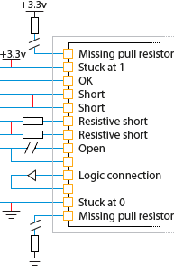
Where two JTAG enabled pins are meant to be connected the test will make sure one pin can be controlled by the other. Where enabled pins are not meant to be connected they are tested for short circuit faults by driving one pin and checking that these values are not read on the other pins. Missing pull resistors and ‘stuck-at’ faults can also be found.
XJTAG’s advanced connection test also checks for other problems such as short circuit faults beyond series resistors as well as automatically testing for faults around devices whose behaviour can be described in a truth table.
What about devices that are not JTAG enabled?
While the main devices, such as processors and FPGAs, are normally JTAG enabled, there will be many devices in every design that are not. DDR, SDRAM, SRAM, flash, MDIO controlled Ethernet PHYs, SPI and I2C temperature sensors, real time clocks, ADCs and DACs are just some examples of such devices.
The connection test will still provide excellent coverage for short circuit faults on the nets linking these non-JTAG devices to JTAG enabled devices; however it cannot check for open circuit faults at either the JTAG device or the non-JTAG device.
In order to add this open circuit coverage it is necessary to communicate with the peripheral device from boundary scan on the enabled device. If communication can be verified, there cannot be an open circuit fault. This type of testing can be very simple, for example lighting an LED and asking an operator to verify it has activated, or more complex, for example writing data into the memory array of a RAM and reading it back.
Is it a lot of work to create an XJTAG test system?
Using the library for standard non-JTAG components installed with XJTAG software, you can get a set of tests up and running for your board with no code development. The XJTAG library contains models for all types of non-JTAG devices from simple resistors and buffers to complex memory devices such as DDR3. Because boundary scan disconnects the control of the pins on JTAG devices from their functionality the same model can be used irrespective of the JTAG device controlling a peripheral.
Most boards already contain JTAG headers for programming or debug so there are no extra design requirements.
Where do I get information about the JTAG in my devices?
In order to run any boundary scan based testing it is necessary to have some information about the implementation of JTAG on the enabled devices on a board. This information comes from the BSDL (Boundary Scan Description Language) files for these devices. BSDL files must be made available by the silicon vendor for a device to be compliant with IEEE Std. 1149.1.
Is JTAG test just used in production?
Not at all. JTAG can be used throughout the product lifecycle including during prototype bring-up, manufacturing test and field diagnostics.
One of the key benefits to boundary scan testing is that the only test hardware required is a JTAG controller. Other production test technologies such as flying probe, automated optical/X-ray inspection or bed-of-nails all require specialised test equipment that will not be available on an engineer’s bench.
Using boundary scan during board bring-up can remove uncertainties – hardware engineers can test prototype boards for manufacturing defects before system testing, and even before firmware is complete. Test systems developed at this early stage of the product lifecycle can easily be reused, and extended for production.
Eight reasons why you should use XJTAG to test your boards
Three simple letters – BGA
An increasing number of devices are supplied in BGA (Ball Grid Array) packaging. Each BGA device on a board imposes severe restrictions on the testing that can be done using traditional bed-of-nails or flying probe machines.
Using a simple four-pin interface, JTAG / boundary scan allows the signals on enabled devices to be controlled and monitored without any direct physical access.
Three more letters – NRE
The non-recurring engineering (NRE) costs of building test fixtures can be prohibitively high. In many cases using JTAG / boundary scan will remove the need for such a fixture, in other cases the fixture can be dramatically simplified resulting in significant cost savings.
Shorter test times
For boards with low production volumes it has always been difficult to justify the cost of test fixture development. In these cases one alternative is flying probe testing; however the test cycle times tend to be high for this technology. JTAG / boundary scan test gives fast test times with no need for a costly fixture.
Lower test development costs
As different processors / FPGAs interact with peripherals in different ways, traditional functional test requires costly custom development for each board. JTAG / boundary scan significantly reduces such development costs because it provides a simplified interface to control the IO pins used to interact with peripherals. This standard interface, which is the same for all JTAG enabled devices, means a generic set of test models can be used, and re-used, when building test systems.
One tool for test and programming
JTAG is often already used as one step in production: programming. By also using JTAG for boundary scan test it is possible to reduce the number of steps and handling operations in the production process.
Production level tests on the engineer’s bench for prototype boards
Traditional test technologies require very large and expensive equipment. The only test equipment required for JTAG / boundary scan testing is a JTAG controller – XJTAG’s XJLink2 controller is a similar size to a PC mouse.
Excellent fault diagnostics
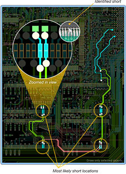
JTAG / boundary scan, unlike functional test, provides high precision fault information to help with rapid repair. XJTAG also provides the capability to view both the physical location of a fault on the layout of the board and the logical design of the area of the circuit in which the fault exists on the schematic.
Recover ‘dead’ boards where functional test would not work
XJTAG boundary scan tests can be run on any board with a working JTAG interface. Traditional functional tests cannot be run if the board does not boot; simple faults on key peripherals, such as RAM or clocks, would be found using JTAG but would prevent functional tests from providing any diagnostic information.

On this page
- How XJTAG uses JTAG/boundary scan to test a board
- What is XJTAG’s advanced connection test?
- What about devices that are not JTAG enabled?
- Is it a lot of work to create an XJTAG test system?
- Where do I get information about the JTAG in my devices?
- Is JTAG test just used in production?
- Eight reasons why you should use XJTAG to test your boards