High-level Guide to JTAG
Introduction
JTAG is an established technology (and industry standard) with a potential that is now becoming fully realised. Connection testing and In-System Programming (ISP) are the two applications most often associated with JTAG, but it has far more to offer.
Though we don’t highlight XJTAG products here, they are designed to harness the full power of JTAG and are able to implement all of the functionality described in this document.
Background
JTAG was conceived to address difficulties in testing circuits using the traditional ‘bed-of-nails’ approach. Modern packaging technologies such as BGA and Chip Scale Packaging limit and in some cases eliminate physical access to pins. (The word ‘pins’ will be used to describe both leaded device connections and BGA solder ball connections.)
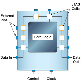
Figure 1 – Simple JTAG device
JTAG overcomes this problem, by placing cells between the external connections and the internal logic of the device, see Figure 1. With the cells configured as a shift register, JTAG can be used set and retrieve the values of pins (and the nets connected to them) without direct physical access.
There’s also an option to sample the data values as they pass between the core logic and the pins during the normal operation of the device.
The JTAG interface adds four extra pins on each device: TDI to input data to the device, TDO to output data from the device, TMS to control what should be done with the data and a clock signal, TCK to synchronise everything.
For a device to be JTAG-compliant, its manufacturer must provide a BSDL (Boundary Scan Description Language) file, which describes how the JTAG aspects of the device work.
If a circuit contains more than one JTAG-compliant device, these can be linked together to form a JTAG chain. In a JTAG chain the data output from the first device becomes the data input to the second device; the control and clock signals are common to all devices in the chain. Figure 2 provides a representation of a simple JTAG chain containing three devices.
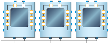
Figure 2 – Simple JTAG chain
Ball Grid Array (BGA)

Figure 3 – BGA device
A BGA package, such as that shown in Figure 3, differs from earlier package technologies in that all of its external connections are made through balls of solder between the bottom face of the device and the circuit board rather than through pins protruding from the side of the device.
The testing of circuits containing BGA packaged devices has been one of the driving forces in popularising JTAG testing. Because the connections between the device and the circuit board are inaccessible both physically and for visual inspection, the only alternative to JTAG for monitoring manufacturing integrity is X-ray inspection. This costly and time-consuming process requires that each board be X-rayed and the images inspected to check each solder ball has been correctly placed, makes contact with the board, but has not spread to cause short circuits. X-Ray provides useful information, but still relies on visual inspection, manual or automated, so cannot be fully relied on to locate all errors.
Against this background JTAG Boundary Scan is more than a useful alternative to bed-of-nails testing; it is a significant money saving tool that can eliminate the need for costly and possibly inconclusive X-ray technology.
Chain Integrity Testing
JTAG testing can be quite basic or very advanced. The most basic form of testing is chain integrity testing, i.e. testing that the JTAG devices that are meant to be in the JTAG chain actually exist.
Most JTAG-compliant devices contain an ID code that can be used to test that the devices are in place and that the JTAG chain is correctly connected. Devices that do not contain ID codes will always return a single bit with a value of 0; so that the JTAG chain can be tested for the correct sequence of devices with, and without ID codes.
Connection Testing
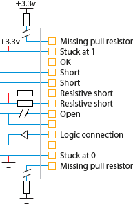
Figure 4 – Connection Test Example
The connection or interconnect test checks the connections around JTAG enabled components in a circuit. These connections, known as nets, can have faults in four categories; short circuit, open circuit, stuck-at, and pull-resistor faults. Examples of these faults are shown in Figure 4.
A JTAG connection test can only fully check for faults on nets between JTAG-compliant devices, where signals can be set at source and read at the destination to check for open circuit faults. (Nets with just one JTAG enabled connection can still be tested for short circuit faults.) Professional boundary scan tools are able to automate the generation of very comprehensive test patterns to implement connection testing, often with minimal manual intervention.
A connection test is an invaluable tool in the process of manufacturing validation. Each circuit that is produced can be checked for production faults caused by manufacturing errors such as solder shorting connectors on a device. Where BGA devices are involved, and there is little opportunity to visually inspect, or physically probe the connections, the value of a JTAG connection test is clear.
Non-JTAG Device Testing
Non-JTAG-compliant sections of a circuit can also be tested. Inputs to non-JTAG devices can be controlled via JTAG wherever these share nets connected JTAG-compliant devices. Similarly the outputs of non-JTAG devices can be read back via JTAG devices. The designers’ knowledge of the expected operation of the non-JTAG-compliant sections will therefore allow them to construct and execute a tests via JTAG that exercise the functionality of the devices.
This form of testing can be applied either to a single non-JTAG device or to any cluster of non-JTAG devices in the circuit which can be viewed as a functional unit. One important example of this method is memory testing. A sequence of JTAG test signals is created to manipulate the control signals and address and data busses of a memory device so as to write information into memory; a second sequence of test signals is created to read this information back.
In-System Programming
Many modern programmable devices, such as FPGAs and CPLDs, implement JTAG not only to facilitate boundary scan testing, but also with additional functionality to allow them to be programmed after they have been attached to a PCB.
Other devices, such as flash memories, can be programmed indirectly through their connection to devices in the JTAG chain.
The ability to use JTAG to program devices ‘in system’ avoids the need to buy expensive programmers and socket. There is also the advantage of being able to easily update the memory image held on the device.
Design for Test
JTAG can be a valuable tool throughout the lifecycle of a circuit. JTAG can help designers, production test engineers and field test engineers.
Effectiveness depends on the coverage that a suite of JTAG tests is able to achieve. The potential is partly inherent in the circuit but can be maximised by the care taken by the designer in designing for test.
A full set of Design For Test (DFT) guidelines is available from the XJTAG web site. However, as a starting point ensure that all JTAG-compliant devices are properly connected and that an appropriate Test Access Port (TAP) has been designed into the circuit.