BSDL & SVF File Formats
Introduction
With all FPGAs, CPLDs and most 32-bit microprocessors including a feature called “boundary scan”, engineers cannot afford to ignore the benefits this feature provides. Boundary scan allows assembled PCBs to be quickly and easily checked for manufacturing faults, and continues to grow in importance due to the increased use of BGAs, which can be very difficult or slow to check for soldering defects with other test technologies.
The many engineers worldwide who already benefit from boundary scan testing will have downloaded BSDL (Boundary Scan Description Language) files and may also have encountered SVF (Serial Vector Format) commands. Although users rarely need to know the intricacies of either file, an appreciation of their contents and the role they play in boundary scan testing can help engineers better understand what files are needed for such tests to run.
This article provides an overview of BSDL and SVF files and describes their basic functions and features to give readers an understanding of their importance.
Boundary Scan Tests
Boundary scan testing utilises the internal architecture of JTAG-enabled devices to take control of their pins: “boundary scan cells” sit between the device’s normal logic and the package’s pins (or BGA balls) as shown in Figure 1. These additional cells allow the non-power pins to be isolated from their normal functionality and, instead, to be set and/or read by a remote PC connected over the board’s JTAG interface.
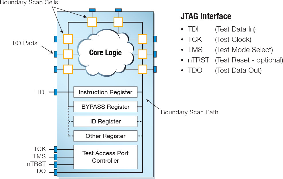
Figure 1 – Boundary Scan Architecture
PC software places the device into its boundary scan test mode and imposes carefully selected test patterns on its pins. The boundary scan cells then record the actual outputs and the resulting inputs on other pins, and the results are sent to the PC software for analysis. In this way, nets suffering from open-circuit, short-circuit or “stuck-at” faults are located, and key devices are confirmed to be operational and correctly placed. This is all without the need to run any software on the board or to have physical access to the pins being checked.
When in boundary scan mode, test patterns and instructions are serially clocked into the TDI pin while the TMS signal manipulates the device’s state machine to control the operation of its internal test logic. The IC contains an instruction register (to hold the boundary scan instruction to be executed) and several data registers, including the bypass register (to allow the boundary cells to be bypassed), and an ID register (that identifies the device); the string of boundary cells is collectively termed the “boundary scan register”.
The state machine is stepped between its various states to allow information to be set or retrieved from these registers, with the instruction register defining which data register is acted upon. The boundary scan architecture, instructions and state machine description are defined by the IEEE 1149.1 standard.
The Need for These Files
For board-test software to be able to control the device in boundary scan mode it needs information on how the manufacturer implemented the architecture. The BSDL file provides this data and can normally be downloaded from the manufacturer’s website. Without the file, it is impossible for boundary scan tests to run, and a manufacturer can only claim IEEE 1149.1 compliance if it is available.
SVF files, in contrast, are one way to record the sequences of state machine transitions and accompanying bit patterns that are used for particular tests. They are not needed to be able to run a boundary scan test, but tools such as XJTAG’s XJDeveloper can accept SVF files and run the routines they define. Because boundary scan can also be used to program a device, manufacturers’ tools can often output an SVF file for in situ programming.
Both files are created in documented ASCII text formats to allow the information to be human readable as well as freely transferable between different vendors’ tools.
Inside a BSDL File
BSDL files are based on the syntax and grammar of VHDL (Very high-speed integrated-circuit Hardware Description Language). They describe those aspects of the boundary scan implementation that aren’t defined by the standard: for example, it provides the length of the instruction register (which is set by the device manufacturer), but not the length of the ID register (which the standard mandates is 32 bits long). It gives information on which boundary scan cells connect to each pin, details of various registers, and a description of the boundary scan cells themselves.
Figure 2 shows the main elements of a BSDL file (for simplicity, not all features are shown).
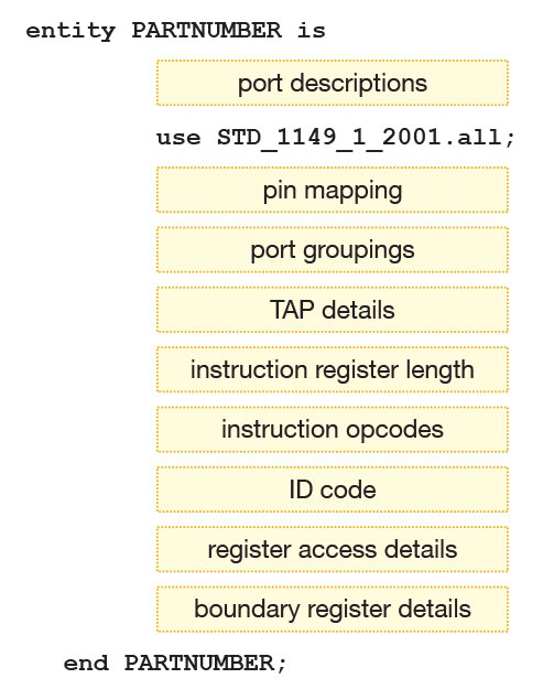
Figure 2 – Main elements of a BSDL file
Port Descriptions
This section of a BSDL file describes all the connections on the device. At this stage, symbolic names are given to each port rather than pin numbers so that definitions created here can be reused for different pinouts without change. Mapping the ports to the device’s physical pins is done later in the file.
Ports that can be used for boundary scan are described as either in, out, bi‑directional or buffer. Because a port name may represent a group of multiple signals, it is also given a dimension: if the port comprises a single signal, the dimension is give as “bit”, whereas if it consists of several, the dimension is stated as “bit_vector” with a figure for the number of signals. This nomenclature may also be used for interlinked power or ground pins. Examples of port descriptions are: “CE: in bit;” and “EXTBUS: out bit_vector (1 to 8);”.
Any connections that cannot be used for boundary scan such as power or analogue pins are defined as “LINKAGE” (in BSDL files created before the 2013 standard). Devices compliant with the 2013 or later versions of the standard differentiate between such pins: for example, a power pin may be defined as “POWER_NEG” and an analogue pin could be “LINKAGE_OUT”.
Pin Mapping
The PIN_MAP attribute now maps each port’s symbolic name to their physical connection on the package and identifies any pins that are not connected. For example, to assign CE to pin 1, VOUT to pin 2 and GND to pin 3, the text string that performs the pin mapping would include: “…CE: 1, VOUT: 2, GND: 3…”.
Port groupings
When multiple pins are needed to carry a single bit of data (for example when differential signals are used), the ports that make up each pair are grouped using the PORT_GROUPING attribute; it also specifies if it is voltage or current signalling.
TAP Details (Test Access Port)
The TAP (Test Access Port) is the name given to the set of JTAG signals (also referred to as the scan port), and the BSDL file includes a set of attributes that tell test tools which port names have been used for those signals. When the port for TCK is defined, its guaranteed maximum frequency is also provided (in Hz) together with details of the logic states in which it can safely be stopped.
Instruction Register Details
Because the length of the instruction register can vary between devices, it is necessary to state its length in the BSDL file. This is done using the “INSTRUCTION_LENGTH” attribute.
Instruction Register Opcodes
An opcode is the name given to the binary sequence needed in the instruction register to perform a particular boundary scan operation. Although the IEEE 1149.1 standard mandates that the BYPASS* instruction must have an opcode consisting of all ‘1’s, no other opcodes are defined and the manufacturer is free to select codes that best suit their design (earlier versions of the standard stated that EXTEST** had to be all ‘0’s, but all-zero opcodes are no longer recommended due to possible problems if a “stuck-at” fault holds TDI low). It is therefore necessary for the manufacturer to supply information on which binary codes have been chosen for each command, and this opcode list is provided in the BSDL file.
An example extract from the relevant attribute string might be: “…SAMPLE*** (0010), EXTEST (0010)…”. Because BYPASS is defined in the standard, it is unnecessary for it to be included in the string, although manufacturers often do so.
Any opcodes that are potentially unsafe to execute because of a risk of damage may also be listed to ensure they are avoided (such opcodes will be identified as “private” instructions).
** The EXTEST instruction inserts the boundary cells between TDI and TDO and allows the clocked-in data to control the state of the device’s pins.
*** SAMPLE inserts the boundary cells between TDI and TDO but leaves the device in its normal operating mode to allow the monitoring of functional data entering and leaving the device.
ID Code
It is not mandatory for a boundary scan device to include an ID register (which provides information on manufacturer, part number and silicon version), but if one has been implemented, the IC’s BSDL file will include matching data. It is defined using the IDCODE_REGISTER attribute, which contains a text string that is normally formatted with comments to make it easily intelligible. Figure 3 shows the format of the ID code description and a typical extract from the BSDL file.
At the commencement of a boundary scan test, the software may check this information against what is hardcoded in the device’s silicon. If they do not match, an error will be reported and the test will stop.
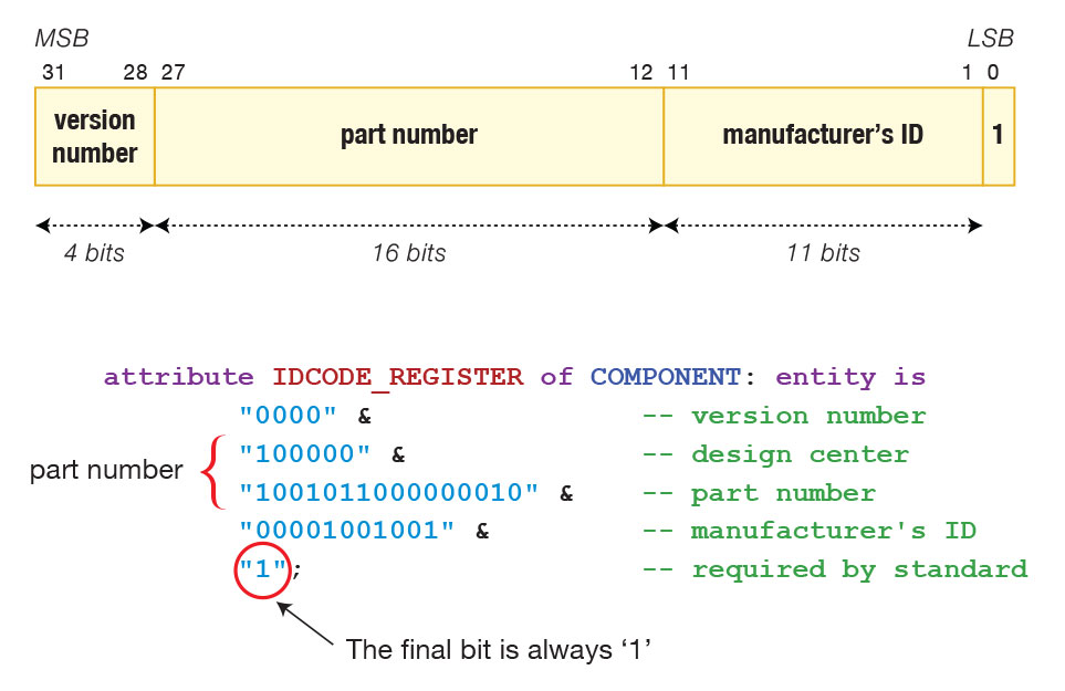
Figure 3 – An example of an ID Code structure
Register Access Descriptions
This section of the BSDL files lists which register will be placed between TDI and TDO for each JTAG instruction. For example, the string “BYPASS (HIGHZ, CLAMP)” informs tools that the BYPASS register will be selected when either the HIGHZ or CLAMP instruction is executed.
Boundary Register Descriptions
The collection of boundary cells is termed the “boundary register”, and the BSDL file describes it in detail. After stating the total number of cells it contains (using the BOUNDARY_LENGTH attribute), the file continues by identifying the different types of cell being used. Figure 4 shows a typical configuration of boundary cells for one pin, and illustrates how a pin can often connect to several boundary cells: in this example, one cell contains the control bit, another the output to be set, and another holds the input value that was read.
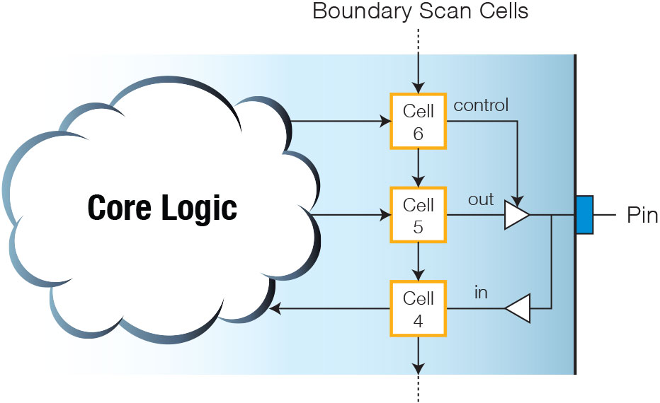
Figure 4 – An example of Boundary Register Cells
For each cell in the register, the BSDL file lists the port it is connected to using its symbolic name, and describes the cell itself and how it is being used. Each entry contains the following information:
- The type of cell. There are many designs for boundary cells: simple ones may be capable only of capturing data whereas other cells may be more universal and capable of updating a pin as well as monitoring it. A simpler cell design might be required where the pin it monitors is particularly sensitive to capacitive loading, such as a clock input. The IEEE 1149.1 standard defines eleven different cell types, designating them BC_0 to BC_10. The IEEE 1149.6 standard (which extends boundary scan to cover AC-coupled signals) adds additional designators AC_0 to AC_10.
- The relevant port it is connected to, using its symbolic name.
- The function of the cell: this describes how the particular cell is being used. IEEE 1149.1 defines several functions including INPUT, CONTROL, CLOCK, and two types of output: OUTPUT2 (for cells driving an output with only high and low states) and OUTPUT3 (for tri-state outputs). In the example of Figure 4, cell 6 is being used as a control cell whereas cell 4 is being used as an input, even though both cells could be of the same design.
- The “safe bit” value: this states the logic value that should be loaded into the cell in any circumstances when it would otherwise be undefined. The value can be set to “X” if it doesn’t matter.
- If the cell’s output can be disabled (such as cell 5 in the example of Figure 4), additional information is supplied that identifies which cell provides the controlling bit, what logic level will disable the output, and what will happen to that output when it is disabled (for example, does it have an internal pull-up or pull-down, or does it become high impedance?).
In the example of Figure 4, the definition might be (ignoring the other cells in the boundary register):
6 (BC_1, *, CONTROL, 0),
5 (BC_1, PINNAME, OUTPUT3, X, 6, 0, PULL1),
4 (BC_1, PINNAME, INPUT, X);
BSDL files include a “use” statement that calls a VHDL package containing information on the cell designs being used. The cell types listed in the IEEE standard are described in standard packages like STD_1149_1_2001 and are called from within the BSDL file by the “use STD_1149_1_2001.all” statement. These filenames indicate the edition of the package to which they refer (1994, 2001, 2003, etcetera). Files for devices supporting IEEE 1149.6 will have an additional use statement to call the package file for cells that support AC-coupling.
As was seen in Figure 2, these statements occur early in the file.
Custom Cell Type Package Files
There may be situations when the manufacturer needs to implement a cell that is different to those defined in the standard package, in which case the BSDL file needs to include information about such custom cells, either by including the data directly in the file or, more usually, by adding a call to a separate VHDL package file. Custom cell package files are called in a similar way to those for standard cells: for instance, to call the file MyPackage, the statement “use MyPackage.all” would be entered.
Because cells can be used in many different ways, the custom cell package will contain several pieces of information for each cell to describe how it will respond to different commands in each mode of use. For example, when used as an input, what will it do when EXTEST is performed? What will the same cell do when the identical command is executed but the cell is being used as an output? All this information is captured in the custom cell type package; Figure 5 shows an extract from the definition of a cell.
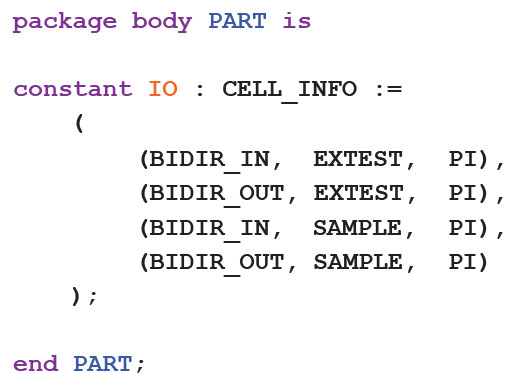
Figure 5 – Extract from a Custom Cell Type Package
Capacitively Coupled Signals
If a device supports capacitively-coupled digital signals and is compliant with IEEE 1149.6, its BSDL file will include additional information about cells with AC capability. The AIO_Pin_Behaviour attribute is used and will include a string that lists which pins support the functionality and, if appropriate, which cell can be used to disable their AC operation. For example, if ports SigA0 and SigA1 support AC signalling and are switched into AC mode by cell 100, it will include the string “SigA0, sigA1 : AC_Select =100”. It may also include a string that defines any associated internal time constants.
IEEE 1149.6 introduced two new instructions, EXTEST_PULSE and EXTEST_TRAIN, that initiate the AC tests. The pulse test is the preferred method, which causes a single pulse to be transmitted, although a train of pulses may sometimes be needed to test particularly troublesome devices. The BSDL file may include attributes AIO_EXTEST_Pulse_Execution and AIO_EXTEST_Train_Execution to provide any related timing requirements.
Compliance Pins
There are situations when a manufacturer may choose to design their device so that its JTAG pins only support the IEEE 1149.1 standard in test mode: at other times, for example, those pins may be reassigned to other functions, or the device may simply ignore JTAG commands.
The standard demands that such ICs must have one or more pins that can be used to force it into IEEE-compliant operation. The BSDL file for such devices will include the COMPLIANCE_PATTERNS attribute to identify the bit pattern that must appear on those pins to switch functionality.
File Formats for Representing Boundary Scan Bit Patterns
When boundary scan tests are run, serial data sequences are clocked into the TDI pin of a JTAG device. The JTAG control signal, TMS, allows these sequences to step the device’s state machine between different stable states and to scan data through the chain; an SVF file is one way to represent these sequences in ASCII text. It allows a file to be created that is agnostic of the tools that will use it, making it a suitable format for files that will be used to program a device, or for when data needs to be transferred between different vendors’ tools.
SVF sequences are purely sequential and lack support for conditional statements. It is therefore not possible to create loops, and familiar constructs such as those using FOR statements are not supported, often leading to large file sizes. SVF files can, however, be a good medium for device programming.
An alternative format is STAPL (Standard Test and Programming Language), which is the standardised version of the earlier JAM™ language created by Altera, and is documented in JEDEC’s JESD-71 standard. STAPL permits loops and other flow control methods, frequently making its file sizes smaller and its execution time shorter. It also supports the polling of devices for their status and therefore does not require the fixed delays often associated with SVF file sequences.
Inside an SVF File
An SVF consists of a sequence of commands as illustrated by the example of Figure 6. In this section, we shall consider the main commands that make up an SVF file.
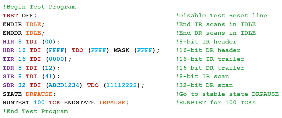
Figure 6 – Example of a Simple SVF File
SVF Commands
The main SVF commands are as follows:
- SIR (Scan Instruction Register): specifies the sequence to be applied to the target device’s instruction register. As well as including the value to be inserted (in hexadecimal), it can also include the expected output from TDO ready for comparison. Masks can be included that should be applied during the comparison if certain bits in the sequences need to be ignored (for example to allow for bits that come from other devices in the JTAG chain, or to ignore ones that are unpredictable such as those originating from an asynchronous clock or from floating inputs).
- ENDIR: specifies the state in which the state machine is to be left at the end of an instruction register scan. These states can be IDLE, RESET or IRPAUSE. An example of using this statement is: ENDIR IDLE.
- SDR (Scan Data Register): specifies the test pattern to be applied to the other target register(s). As well as including the value to be inserted (in hexadecimal), it can again include the expected TDO output ready for comparison and any applicable masks.
- ENDDR: specifies the state in which the state machine is to be left at the end of a data register scan. These states can be IDLE, RESET or DRPAUSE.
- STATE: this command is used to move the device’s state machine from one stable state to another and may include transitions through intermediate states. For example, to go to its IDLE state via the RESET state, the statement would be: STATE RESET IDLE.
- PIOMAP & PIO: SVF files can work with parallel test vectors, and the PIOMAP command is used to define which ports are being used in that way. Each one is identified using its symbolic name, and information is provided on the pin direction (input, output or bi-directional). For example, “PIOMAP (IN a IN b IN c)” defines pins a, b and c as parallel inputs. The PIO command can then be used to specify the parallel test pattern to be applied: for instance, following the previous PIOMAP command by “PIO (HLZ)” will set the pin with name “a” to a high level, the pin “b” to a low level, and the pin “c” to its high impedance state.
- RUNTEST: places the device’s state machine into the run state for a certain length of time or number of clock pulses.
- TRST (Test Reset): controls the optional test reset signal.
- FREQUENCY: specifies the maximum TCK frequency (in Hertz) to be used from then on. If this command occurs without a parameter for frequency, it will be set to full speed.
Whenever an SVF file is used to perform operations on a chain of multiple JTAG devices, there will be several bits within the sequences that are not relevant to the target device. For example, an SIR instruction may first need to shift non-targeted devices in the chain into BYPASS so that only the desired device executes the instruction.
As the chain length increases, needing to repeatedly insert these additional sequences can dramatically enlarge the SVF file. To minimise this, headers and trailers may be used to define bit patterns to be applied to the start or end of every scan sequence. The HDR and HIR commands are used to automatically append a sequence to the start of the data register and instruction register sequences respectively. The equivalent TDR and TIR commands do the same for trailing sequences.
Summary: The Importance of BSDL, SVF & STAPL Files
Because a BSDL file is the medium for describing how an IC’s boundary scan architecture is implemented, it is essential to obtain that file if boundary scan testing is to be performed. It contains information such as the size of the instruction register, the binary codes that equate to the different instructions, which of the optional commands are supported, and details of each cell used in the boundary register.
SVF and STAPL files, in comparison, are not needed to run a boundary scan test, but are ways to list the state machine transitions and bit patterns that make up a particular test or function. Because boundary scan can be used to program devices, manufacturer’s tools can often generate these files as a means of in-circuit programming.
Boundary scan testing provides a powerful method to pinpoint soldering defects, including those in inaccessible locations such as beneath BGAs. Test tools such as those from XJTAG provide engineers with an intuitive user interface that allows such tests to be designed and run without the need for a detailed knowledge of the content of its associated files.