Traceable by Design: Preparing Altium Projects for XJDeveloper Success
If you are you working with hierarchical schematics in Altium and you’re preparing your board data for import into XJDeveloper, there are a few key things that can help streamline the process, making test development and debugging faster and less error-prone. These factors are even more important if your design includes repeated blocks, like the controller board inside the XJLink-PF40.
Here’s how we made our schematics more developer-friendly and test-ready with practical tips and examples from the XJLink-PF40.
Export each channel as a separate page
The I/O for each of the XJLink-PF40’s front connectors are all built using copies of the same schematic blocks:
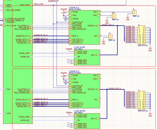
Some of these blocks (eg, U_BANK_IO) contain additional repeated blocks:
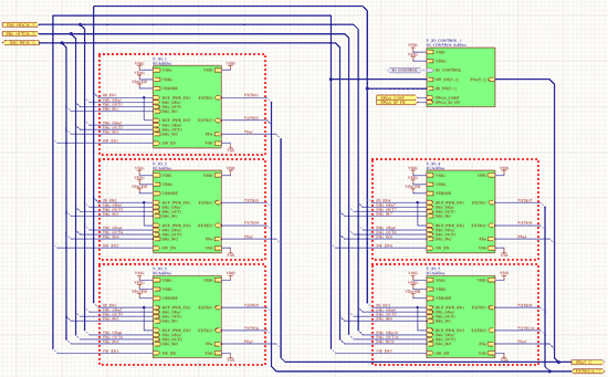
To make the resulting schematics more readable (and hence easier to trace and debug), we export each instance of a repeated block as its own page, rather than exporting a single generic symbol.
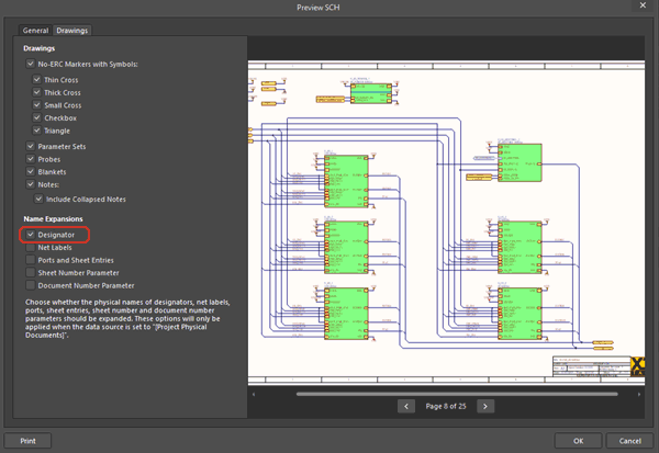
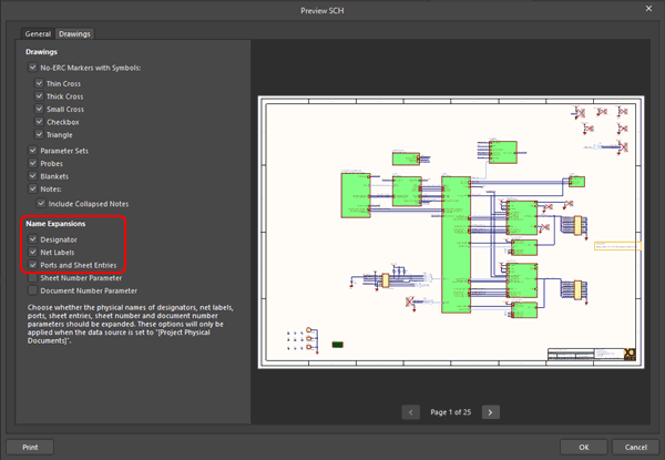
To do this, select “[Project Physical Documents]” rather than “All SCH Documents” in your output job file. This produces a compiled version with all parameters filled in and hierarchies resolved:
![select “[Project Physical Documents]” in output job file](https://www.xjtag.com/wp-content/uploads/appnote-altium-xjdeveloper-fig3.gif)
And when configuring the output, make sure “Designator” is enabled under “Name Expansion”:
Why this matters:
- All the schematic sheets, and components within those sheets, get their own unique reference designators, preventing mismatches when searching.
- Developers can trace specific nets and components directly in the schematic.
- It’s much easier to isolate and fix issues during test development and validation.
Keep Naming Consistent
When using hierarchical sheets, consistent naming conventions are essential.
In the XJLink-PF40, we used descriptive sheet symbol names (e.g. U_BANK_IO_1, U_ADC_BANK_1) and kept port names identical across repeated blocks. This preserves net continuity and reduces confusion.
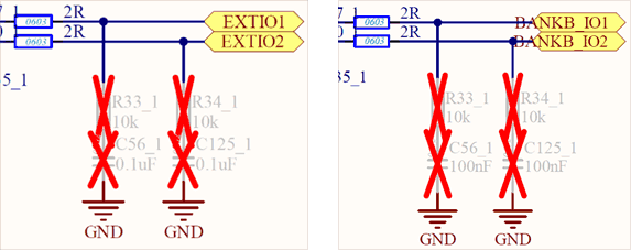
When generating the schematic output, you can configure the project to use the true net names throughout the design. This keeps the net names consistent as you move through the hierarchy, making it much easier to trace nets through the schematic. The trade-off is that the exported schematics can look a little messier, due to the longer net names:
This can be enabled in the schematic export configuration screen:
Don’t use “Merge Net-Tie Nets” in ODB++
Altium’s ODB++ export includes an option to “Merge Net-Tie Nets”. This option combines nets that are connected by a tie (a component to short them together), turning them into a single net in the netlist:
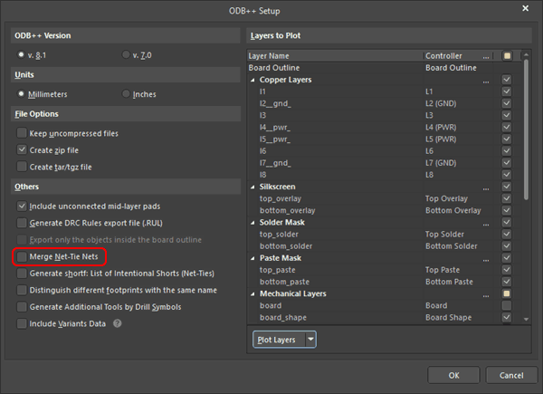
Using this feature might seem useful as it removes net ties from the BOM by merging the nets, but this causes problems:
- The exported netlist will include nets that don’t exist in the schematic.
- These phantom nets can’t be traced through the schematic or layout as their names don’t exist in the original design.
- XJDeveloper will struggle to correlate net names, leading to inaccurate test coverage
- It introduces ambiguity in test reports and can make debugging more difficult
For the XJLink-PF40, we explicitly disabled this option to preserve a one-to-one mapping between schematic nets and the exported netlist. This made all test nets fully traceable back to the original design.
Export a XJDeveloper Preferred Netlist
When exporting netlist and layout information for XJDeveloper projects, we recommend customers use ODB++ (in zip format) whenever possible. This format contains both netlist and layout information and can be generated by almost all CAD tools.
If you can’t use ODB++, XJTAG supports automatic parsing for over 100 netlist formats including RINF, Protel, PADS-PCB, Cadence Allegro, P-CAD, GenRad, BoardStation (Mentor), Zuken, Protel V2 and many others.
Conclusion
Applying these guidelines when working with hierarchical schematics in Altium, especially in designs with repeated blocks like the XJLink-PF40, can make your test development in XJDeveloper faster, more accurate and far less frustrating!
- Export each channel as its own schematic page
- Keep naming consistent across sheet symbols and ports
- Avoid merging net-tied nets in ODB++
- Choose the ODB++ netlist format to include layout information
By following these steps, you’ll not only simplify debugging and validation but also ensure that your schematic data translates seamlessly into robust boundary scan tests.
Whether you’re building complex multi-channel systems or refining a single board, these strategies help bridge the gap between design and test with clarity and confidence.