Using XJTAG with Differential Signals
Introduction
Differential signalling such as LVDS is now supported by many FPGA vendors and can cause some problems when these signals are used in JTAG tests. This article attempts to describe some of the pitfalls and remedies associated with using differential signalling paths with JTAG. To use FPGAs to test differential signals within JTAG depends on a number of different settings. If both the FPGA pin and the transceiver device are 1149.6 compatible, then 1149.6 standard compatible tests can be done on the nets.
FPGAs driving differential signals
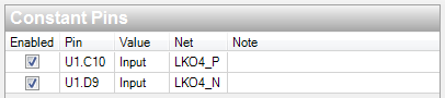
Many differential signalling outputs of FPGAs are not available until the device is fully configured and the outputs have become enabled. However, JTAG activity will take place when the device is unconfigured and the outputs will usually default to a conventional CMOS driver using a common output voltage. Care should be taken that differential receivers attached to these output pins can safely handle the default output voltage generated by the FPGA. If the receiver cannot handle these voltages, the FPGA should be prevented from driving the differential nets, by using the CONSTANT PINS section of the project setup. In the example shown below, the FPGA (U1) is prevented from driving the differential signalling pair connected to pins C10 and D9.
FPGAs receiving differential signals
An FPGA differential signal receiver will not usually be able to detect the small signalling levels driven by a differential transmitter when in its unconfigured state (such as when JTAG is active). Thus JTAG tests which require input on these pins will not usually be possible.
Other JTAG-enabled differential transmitters
Many JTAG-enabled devices with dedicated differential transmitter pin pairs have only one JTAG control cell attached to each pair of transmitter signal pins, so driving one of these pins high will usually result in the paired signal being driven low and vice-versa. This should be borne in mind when designing tests using such pins. As there is only a single control cell for a pair of pins, there will therefore be no BSDL description for one of the pins of each pair, and any attempt to drive this pin will cause a run-time error.
FPGA configuration
Ideally for JTAG testing then, the FPGA should be unconfigured to give the best test coverage on each pin. This however reduces the functionality of the FPGA, and would remove the devices ability to test differential signal inputs. To overcome this and be able to test differential signals the FPGA can be configured with a very basic image which configures the differential pairs, while leaving the majority of the pins unconfigured for JTAG testing.
Altera provide instructions for creating the linked BSDL file which can be used within the tests, which will correctly represent this as a differential pair: BSDL Files Generation in QII.doc.
NB: Configuring a new image may however restrict JTAG access over more pins than intended.