Capabilities and Limitations of Logic Devices in an XJTAG Test System
Introduction
In circuits containing Logic Devices an XJTAG test system will automatically attempt to exercise those devices in the connection test, and may also use the devices to carry out SET statements in your XJEase Test Device Files. This is a highly useful feature which means the test designer does not usually need to worry about the connections between devices in the JTAG chain and the device being tested. However the automatic handling of Logic Devices does have certain limitations.
Automatic set-up of logic gates
Consider Figure 1, showing simple scenarios using AND gates. Looking first at Gate 1, a SET statement in XJEase that attempted to read the Test Device pin can be carried out by setting the output of the JTAG device connected to pin B of the AND gate high, so that the input on pin A would then control the output at pin C. By reading pin C on gate 1, the value at pin A and thus on the Test Device can then be inferred. XJEase works this out and performs the operation automatically.
This automated behaviour means that in XJEase SET statements, it is possible to read a bus on a Test Device even if that device is connected to Logic Devices rather than directly to boundary scan enabled pins.
Looking next at Gate 2, if a SET statement is used to write to the Test Device on the right, XJEase will automatically set up the inputs to produce the required output on pin C.
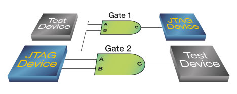
Although XJEase can use Gates 1 and 2, the connection test cannot prove the correct operation of the logic in either of these cases. For Gate 1 the voltage at pin A is not known by the connection test, so it is not possible to drive pin B from boundary scan and know what value should be read at C. For gate 2, output pin C cannot be read from boundary scan so it is not possible to check whether the values driven on the inputs cause the expected output (although connection test will drive the gate to check all its pins (including the output) for short-circuit faults to other nets.
Limitations of automatic setup
In Figure 2, the pull resistor adds an extra complication to the scenario, and XJEase can no longer cope automatically with reading or writing through Gates 3 and 4.
Pin A of each logic gate is connected to both a Test Device and a pull-up resistor, so that when the Test Device is inactive, the input to the AND gate is high.
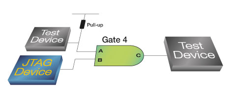
Figure 2 – More complicated scenarios
In this situation, there are two ways that Gate 3 could be used:
- when the Test Device is not driving, the output pin C of the AND gate can be controlled from the JTAG pin connected to pin B
- the value of the input pin A on the Test Device can be read by setting a known value on the input pin B and then reading pin C
Both of these options appear to be achievable. By ensuring the Test Device is inactive, so the pull-up keeps input A high, the first operation can be achieved while keeping input B high allows input A to be monitored by reading the value of output C.
Unfortunately it is not currently possible for XJTAG’s automatic Logic Device support to perform both 1) and 2). With both Test Device and pull-resistor configured only 2) can be achieved as there is no way to tell XJTAG that the pin on the Test Device is not driving input A. Without this information XJTAG does not know that the pull resistor will provide the high level at this node which would allow input B to control the output. Similarly on gate 4, if a SET statement attempted to set the output net (expecting it to set the desired value on pin B), XJEase would report that it is unable to set the value.
Work-arounds
Keeping the AND gate’s logic definition
There are two ways in which situation 1) above can be made to work. Either the Test Device could be recategorised as an Ignore Device, or the pull-up resistor could be categorised as a direct connection. With the Test Device ignored XJTAG would interpret the pull resistor as being the only device controlling the net and equally with the resistor defined as a connection the net would be interpreted to be part of the power net and therefore always high. Unfortunately both of these solutions would prevent the pin on the Test Device from being read, meaning that 2) can not be performed.
Fundamentally, the reason that the two functions can’t both be done using the automated logic is that XJTAG does not have enough information – it has no knowledge of when the test device is going to drive pin A on the logic gate, and when it is inactive. There is no way in the current version of XJTAG to give it this information.
Bi-directional work-around – Modifying the logic device
Providing that it is possible to control when the Test Device is outputting, it is, however, possible to work around this problem by ‘manually’ describing some of the operation of the AND gate. In this instance Gate 3 could be categorised as a simple buffer with an input at pin B and an output at pin C; this would allow the connection test to check that the two JTAG pins can exercise some of the functionality of the gate. In the Test Device file the bus for the pin connected to the AND gate could then be defined specifically in terms of the output of that gate; there would also have to be an extra bus that contained an specific reference to the boundary scan controllable input at pin B. At the start of the test the bus relating to pin B would be set high so that the value read at C would be controlled by A.
Summary
This example shows both the capabilities and limitations of XJTAG’s automatic Logic Device support, and hopefully shows the kind of solutions which can be found if your circuit design cannot currently be automatically supported. If you feel you are facing a situation like this and you cannot find a solution, please contact Support – and we will try to help you work around the issue.