
XJFlash Module
The fastest way to program flash
XJFlash is an advanced FPGA-based module that uses JTAG for accelerated in-system programming (ISP) of flash memories, supporting all serial and parallel flash devices.
Using the FPGA on your board you can achieve flash programming speeds up to 50 times faster than those of conventional boundary scan techniques, usually reaching the flash memory’s maximum speed.
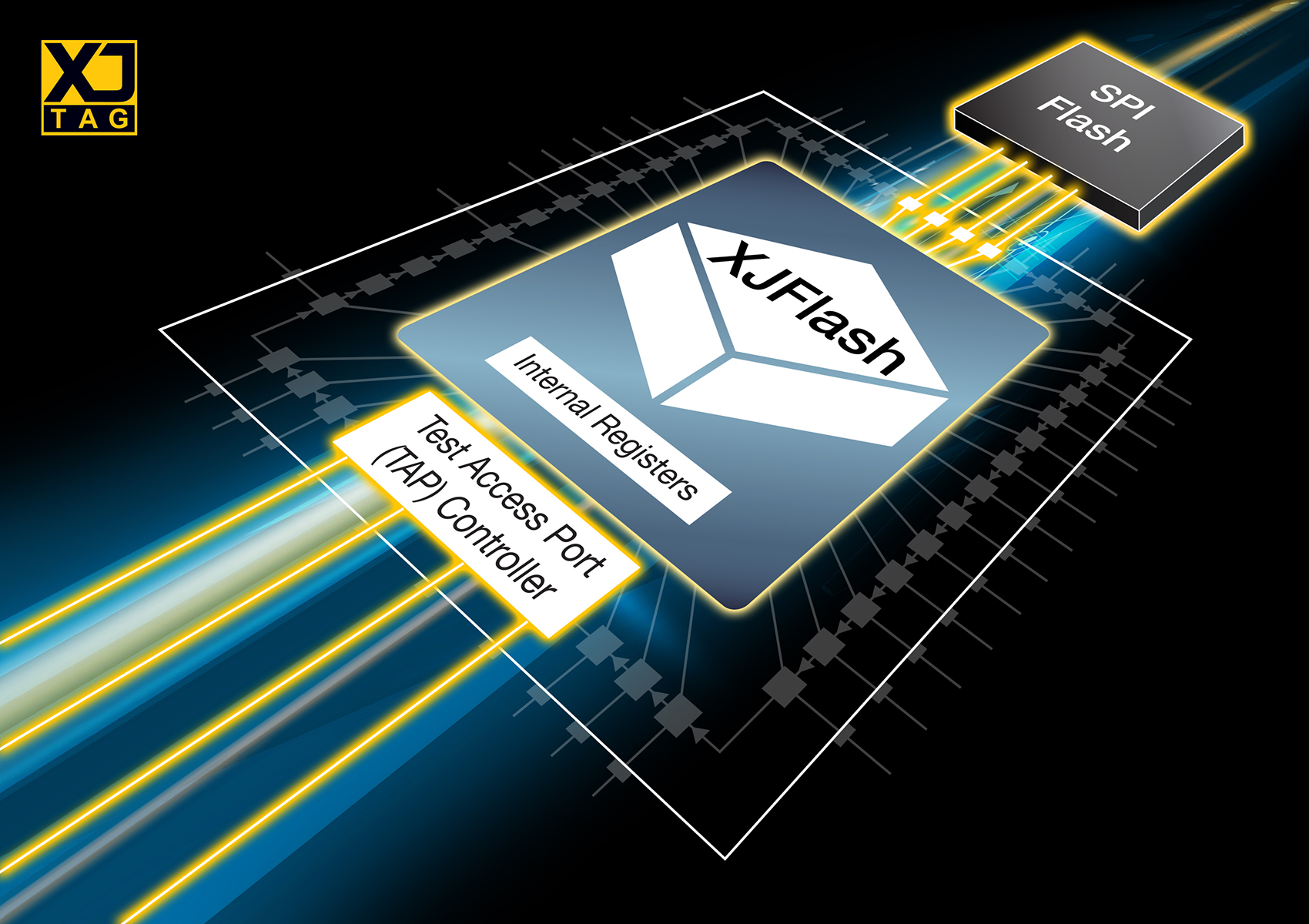
XJFlash automatically generates customised programming solutions for the flash memory devices connected to FPGAs and FPGA SoCs (such as AMD Xilinx Zynq™ and Altera Cyclone® V) on your board. The functional capabilities of the FPGA are harnessed to provide the fastest possible programming speeds, without requiring you to do any FPGA development.*
If your flash memory is connected to an FPGA from Altera (Intel), AMD (Xilinx), Microchip (Microsemi) or Lattice, XJFlash uses the FPGA’s standard JTAG port to offer an in-circuit programming alternative to a SPI programmer or parallel flash programmer. XJFlash supports all SPI modes (single-bit, dual, quad, QSPI, and octal) as well as parallel NOR flash devices.
Whether you have a single flash memory or multiple devices to program, and whether you have devices connected in series to expand the address space, or in parallel to make a wider data bus, XJFlash can speed up your programming operations. XJFlash programming can be easily integrated into your XJTAG test system using XJDeveloper, and then run on any XJRunner system as part of a boundary scan test project.
*A licensed version of the relevant FPGA manufacturer’s tools will be required during the configuration of XJFlash. Free versions are sufficient for many devices.
Benefits
Cut flash programming times
Programming speed often limited by flash device write speed. Intelligent erase functionality only performs erase operations when necessary
Use single controller and single project to both program and test
No need for additional equipment or to swap plugged in JTAG controller
XJFlash doesn't need a special licence to run
An XJFlash licence is only needed to generate the project. To run, just use XJRunner
Wide range of flash device types
SPI, QSPI, parallel NOR flash devices supported. Support for NAND devices available on request
No FPGA development required
XJFlash will make use of the FPGA manufacturer’s tools but this use is scripted, the user does not have to know how to use them
Custom devices, configurations and operations
Different configurations of flash chips, programming files and indirectly connected flash devices can be supported.
Custom development
The most common use of XJFlash is programming the SPI/QSPI NOR flash used to configure an FPGA, but XJFlash can also be used for standalone programming tasks including via direct access to I²C and SPI busses or custom protocols such as Microchips ICSP.
The required connections do not need to come from an FPGA on the target board. If the protocol signals are available on a header, it should be possible to use XJFlash to achieve fast programming as part of an XJTAG solution.
Performance
Minimum theoretical time for conventional boundary scan: 35 minutes.
Total XJFlash run time: 10.5 s to 32.6 s.
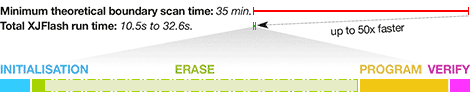
XJFlash will automatically step through four stages each time a flash device is programmed:
Initialisation – The FPGA connected to the flash is configured with the XJFlash image required for the target board. Example time: 2.1 s.
Erase – The flash can be erased using one of two algorithms. The basic erase will simply erase all blocks within a defined range (this may be the whole flash or just the space needed for the image to be programmed). The more intelligent erase will use the fact that it is quicker to read the flash than to erase it; as such it reads from each address and only starts erasing if some data is found. This step can be skipped if it is known that the flash will always be blank before it is programmed. Example time – intelligent erase enabled: 0.9 s with a device already erased, to 23 s with a fully programmed device (limited by erase time of device).
Program – Data from the target images is streamed into the FPGA through its JTAG port. The FPGA then programs this data into the connected flash(s). Multiple files can be specified and programmed at defined offsets. This step can be bypassed if only verification is required. Example time: 6.2 s (limited by the programming speed of the device).
Verify – The verification checks every byte in the flash against the specified file(s), ensuring there are no data bit errors. This step can be bypassed if only programming or erasing is required. Example time: 1.8 s with TCK at 10 MHz, reducing to 1.3 s with TCK at 20 MHz.
Example Timings Using an AMD Xilinx Zynq™ 7000 series SoC
A 256 Mbit file can be programmed into a SPI NOR flash and verified in around 46 s, depending on the TCK speed and the memory type being used*; 32 Mbit of code takes just over 7 s.
Adding an initial erase cycle adds only 3.1 s for an empty 256 Mbit flash, or 54 s for a full one. That drops to 0.4 s and between 6.5 and 9.2 s respectively for a 32 Mbit device.
* TCK = 66 MHz, pseudorandom data file. Time varies with flash type.
Example Timings Using an AMD Xilinx Zynq™ UltraScale+™ series SoC
A 256 Mbit file can be programmed into a SPI NOR flash and verified in around 42 s, depending on the TCK speed and the memory type being used**; 32 Mbit of code takes 7 s.
Adding an initial erase cycle adds only 2 s for an empty 256 Mbit flash, or 57 s for a full one. That drops to 0.3 s and 6.9 s respectively for a 32 Mbit device.
** TCK = 30 MHz, pseudorandom data file. Time varies with flash type.
Requirements
In order to use XJFlash, all of the data bus, address bus and control signals on the flash device must be controllable from an FPGA. In most cases they will be controlled by an FPGA on the UUT. The flash device can be a configuration PROM for the FPGA, or a flash device connected to any general purpose I/O pin. Connections between FPGA and flash can be direct, indirect, dedicated or shared:
Direct connections – YES


The flash is directly connected to the FPGA.
Indirect connections – YES

- The flash is connected to the FPGA via a buffer
- Some of the address signals are shared with the data signals and connected via a latch.
- There is another configurable device, such as a CPLD between the flash and the FPGA.
Shared connections – YES

The flash is connected to the FPGA in one of the modes described above but these connections are shared with another device (such as a processor).
No connections – YES (with design changes)

If your design contains an FPGA but the flash is not connected in any of the configurations described, it may be possible to use spare pins on the FPGA to establish connections to the flash. These connections would not be used in the mission mode of the board but would allow you to use XJFlash to perform fast flash programming. If your FPGA is already connected to the same address/data bus as the flash then this may not require many extra signals.
No FPGA – Not directly

Unfortunately, it is not possible to use XJFlash if there is no FPGA. However, if it is possible to bring the connections of the flash to a header or test points on the board, XJFlash fast programming can be used via those connections using an XJAccelerator card.
Alternatively, it may be possible to do fast flash programming using the debug interface on a processor – please contact us to see if you can use this approach on your board.
Compatibility
Supported FPGA families
- Altera – Arria GX, Arria II GX, Arria II GZ, Arria V, Arria V GZ, Arria 10, Cyclone, Cyclone II, Cyclone III, Cyclone III LS, Cyclone IV E, Cyclone IV GX, Cyclone V, Stratix, Stratix GX, Stratix II, Stratix II GX, Stratix III, Stratix IV, Stratix V, Stratix 10
- AMD (Xilinx) – Artix-7, Artix UltraScale+, Kintex-7, Kintex UltraScale, Kintex UltraScale+, Spartan-3, Spartan-3A, Spartan-3E, Spartan-6, Spartan-7, Versal, Virtex-II, Virtex-II Pro, Virtex-4, Virtex-5, Virtex-6, Virtex-7, Virtex UltraScale, Virtex UltraScale+, Zynq-7000, Zynq UltraScale+
- Lattice – MachXO2, LatticeECP3, LatticeXP2
- Microchip (Microsemi) – IGLOO2, ProASIC3, ProASIC3E, ProASIC3L, SmartFusion2
This list is continuously growing, so contact us for the latest details.
All trademarks are the property of their respective owners.
Flash Programming Solutions
| XJExpress | XJExpress-FPGA | XJDeveloper & XJRunner | |||
| Native | XJFlash | XJDirect | |||
|
Performance |
|||||
|---|---|---|---|---|---|
| SPI NOR Flash Indicative Speed | 12Mb/s | 12Mb/s | 10kb/s | 12Mb/s | 3Mb/s |
| Speed Limiting Factor* | Target Memory | Target Memory | Boundary Scan | Target Memory | Debug Interface** |
|
Connection |
|||||
| Controller Connection | USB | USB, PXI | USB, PXI, ATE | USB, PXI, ATE | USB, PXI, ATE |
| Programming Type | Direct | Indirect-FPGA | Indirect Boundary Scan, Direct | Indirect-FPGA, Direct*** | Direct, Indirect-Processor |
| Intermediate Devices | None | FPGA | None, JTAG device | FPGA, None | None, Processor |
| Board Access | N/A | JTAG | N/A | JTAG*** | JTAG, SWD |
| Flash Interface Bus | SPI† | SPI†, Parallel, eMMC | SPI†, Parallel, I2C, eMMC, JTAG | SPI†, Parallel, eMMC | Internal, External SPI†, Parallel, I2C, eMMC |
|
Supported Devices‡ |
|||||
| SPI NOR Flash | ✓ | ✓ | ✓ | ✓ | ✓ |
| Parallel NOR Flash | ✗ | ✓ | ✓ | ✓ | ✓ |
| NAND Flash | ✗ | ✓ | ✓ | ✓ | ✓ |
| eMMC | ✗ | ✓ | ✓ | ✓ | ✓ |
| MRAM | ✗ | ✓ | ✓ | ✓ | ✓ |
| FRAM | ✗ | ✓ | ✓ | ✓ | ✓ |
| NVSRAM | ✗ | ✓ | ✓ | ✓ | ✓ |
| PCM | ✗ | ✓ | ✓ | ✓ | ✓ |
| EEPROM | ✗ | ✓ | ✓ | ✓ | ✓ |
|
Interface & Control |
|||||
| Hardware Controller Included | ✓ | ✓ | ✗ | ✗ | ✗ |
| Application GUI | ✓ | ✓ | ✓ | ✓ | ✗ |
| Command Line Interface | ✓ | ✓ | ✓ | ✓ | ✓ |
| Control by API | ✗ | ✓ | ✓ | ✓ | ✓ |
| Logs | ✗§ | ✓ | ✓ | ✓ | ✓ |
| Lockable Project Format | ✓ | ✓ | ✓ | ✓ | ✓ |
| Integrated Into XJTAG Testing Suite | ✗ | ✗ | ✓ | ✓ | ✓ |
|
Configuration |
|||||
| Erase/Program/Verify Configuration | ✓ | ✓ | ✓ | ✓ | ✓ |
| Customisable Configuration | ✓ | ✗ | ✓ | ✓ | ✗ |
| Register Configuration | ✗§ | ✓ | ✓ | ✓ | ✓ |
| Auxiliary Pin Control | ✗§ | ✓ | ✓ | ✓ | ✓ |
| Auxiliary Device Control | ✗ | ✓ | ✓ | ✓ | ✓ |
| Target Configurations Included With Purchase | All | 1 | All | All | 1 |
| Full Device Library Access | ✓ | ✗ | ✓ | ✓ | ✗ |
|
Support |
|||||
| 1 year product warranty | ✓ | ✓ | ✓ | ✓ | ✓ |
| 1 year support and maintenance from XJTAG engineers (can be extended) | ✗ | ✗ | ✓ | ✓ | ✓ |
* in normal use, other limiting factors may cause restrictions for specific device types and configurations
** Ethernet or other fast buses can be used via XJDirect for faster programming
*** or directly with an XJAccelerator accessory board
† single, dual, quad and octal supported
‡ not all memory types are listed, please contact us for specific enquiries
§ coming in Q2 2026, available as a free upgrade
Any more questions
Recommended system requirements
Intel® Core i3, i5, i7 processor or equivalent (any generation).
Microsoft® Windows® 11.
8 GB of RAM.
Flexible Licensing Options
Hardware licence
Held in the JTAG controller so you can install XJTAG on any number of PCs.
Network licence
Held on a networked license server available from anywhere in the world.

Configure your products


Take a Free Trial of XJTAG software & hardware products
30 days of discovery with full features
Any questions? Contact us