XJFlash — 超高速フラッシュ書き込みツール

XJFlashは先進的で革新的な、JTAG経由の各種フラッシュデバイスのインシステムプログラミング(ISP)技術です。

XJFlashを使えば、バウンダリスキャンによる従来方式に比べてフラッシュ書き込みを50倍までスピードアップ可能です。

XJFlash データ資料 お問い合わせ 評価版

書き込み手順 – 自動生成

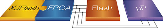
XJFlashなら、基板上のFPGAに接続されたフラッシュデバイスごとにカスタマイズされた書き込み手順を自動生成することができます。

XJFlashは可能な限りの書き込みスピードを実現するために、FPGAが持つ機能をフル活用します。人手による設計なしで最高性能が得られるように、各々のFPGAとフラッシュデバイスの組み合わせごとにカスタマイズされたロジックを自動生成します。*

SPI、QSPI、パラレルNORといったフラッシュデバイスの種類、またIntel(Altera)、Xilinx、Microsemi、LatticeといったFPGAのメーカーを問わず、XJFlashは基板に最適化された書き込み手順を提供します。

*XJFlashの設定時にはFPGAメーカーによる正規ライセンス版ツールが必要になります。多くのデバイスでは無償版でも使用可能です。

テストとの統合

XJFlashはXJTAG開発システムと互換性がありますので、XJRunnerのテストプロジェクトの一部として書き込みを実行できます。

さまざまな構成のフラッシュデバイスへの書き込み

単一デバイス、あるいはアドレス空間を拡げる直列接続やバス幅を拡げる並列接続等、いずれの構成でも、書き込み作業の高速化のためにXJFlashを使うことができます。

カスタム開発

XJFlashはI²CやSPI、あるいはMicrochip社のICSPのような独自プロトコルのバスへのアクセスにも対応可能です。

またこれらのバスにターゲット基板上のFPGAが接続されている必要はありません。XJTAG開発システムの一部として、基板上のヘッダ経由で高速書き込みが可能です。

XJFlash所要時間の例

バウンダリスキャンによる従来方式での理論上の最短時間: 35分.
XJFlashの場合: 10.5~32.6秒.

XJFlash programming stages

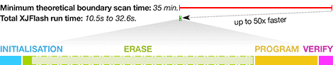
XJFlashは書き込みのたびに自動的に次の四つのステップを実行します。

  初期化 – フラッシュデバイスに接続されたFPGAにターゲット基板向けのXJFlashデータが書き込まれます。

所要時間: 2.1秒

  消去 – フラッシュデバイスが2種類のうちいずれかのアルゴリズムを用いて消去されます。基本モードでは定められた範囲のブロック(これはデバイス全体の場合もあ るし、書き込むデータに必要な領域のみの場合もあります)を単純に消去します。インテリジェントモードでは消去より読み出しのほうが速いという特性を応用 して、何らかのデータが書き込まれている箇所だけを消去します。なおデバイスがブランクであると分かっている場合は消去ステップを省略することもできま す。

所要時間 – 高機能モードを使用: ブランクの場合0.9秒、全領域書き込み済みの場合23秒(デバイスの消去速度に依存します)

  書き込み – JTAGポートを経由して書き込みデータがFPGAに送られます。FPGAはこのデータをフラッシュデバイスに書き込みます。複数のデータファイルをそれぞれの位置に書き込むことも出来ます。このステップを省略してベリファイだけを実行することもできます。

所要時間: 6.2秒(デバイスの書き込み速度に依存します)

  ベリファイ – フラッシュデバイスとデータファイルを1バイトごとに比較して、エラーがないことを確認します。このステップを省略して書き込みや消去だけを実行することもできます。

所要時間: 1.3秒(TCK 20MHz) ~ 1.8秒(TCK 10MHz)

これらの所要時間は Spartan 6 XC6SLX9 を使用して、2MByteのランダムなデータをSPIコンフィギュレーションPROMに書き込んだ場合の数値です。

XJFlashが使えるケース

XJFlashを使用するにはフラッシュデバイスのすべてのデータ、アドレス、制御信号が基板上のFPGAに接続されている必要があります。コン フィギュレーションPROMや汎用I/Oに接続されたフラッシュデバイスなどへも書き込むことができます。なお直接これらの信号線が接続されている場合は もちろん、バッファを経由していたり、別のデバイスと共有バスになっている場合でも使用可能です:

直接接続 – 使用可能

XJFlash Configuration - Direct Connections to FPGA

XJFlash Configuration - Direct Connections to FPGA SoC

フラッシュデバイスがFPGAに直接接続されている。

間接接続 – 使用可能

XJFlash Configuration - Indirect Connections

  1. フラッシュデバイスがバッファを通してFPGAに接続されている。
  2. データバスがアドレスバスを兼ねており、ラッチを通して接続されている。
  3. フラッシュデバイスとFPGAの間にCPLDのような別のデバイスが接続されている。

共有接続 – 使用可能

XJFlash Configuration - Shared Connections

フラッシュデバイスが上記のいずれかの方法で接続されているが、CPUのような別のデバイスとバスを共有している。

無接続 – 使用可能(設計変更が必要)

XJFlash Configuration - No Connections

フラッシュデバイスが上記のいずれの方法でも接続されていない場合でも、FPGAの空き端子にフラッシュデバイスを接続できる可能性があります。こ れは基板の稼働中には使われず、フラッシュデバイスの書き込み時にXJFlashによる高速動作を実現します。またFPGAがフラッシュデバイスと同じアドレス/データバスにあるデバイスであれば、さらに信号線を減らすことができるかも知れません。

FPGAなし – 工夫次第

XJFlash Configuration - No FPGA

残念ながらFPGAが搭載されていない基板ではXJFlashが使えませんが、CPUのデバッグインターフェースを使えば高速書き込みができるかも知れません。詳細についてはお問い合わせください

また別の方法として、フラッシュデバイスの信号をヘッダーから引き出すことができれば、それを通してXJFlashを使うことができます。

互換性

  • Intel (Altera) – Arria GX, Arria II GX, Arria II GZ, Arria V, Arria V GZ, Arria 10, Cyclone, Cyclone II, Cyclone III, Cyclone III LS, Cyclone IV E, Cyclone IV GX, Cyclone V, Stratix, Stratix GX, Stratix II, Stratix II GX, Stratix III, Stratix IV, Stratix V, Stratix 10
  • Lattice – MachXO2, LatticeECP3, LatticeXP2
  • Microsemi – IGLOO2, ProASIC3, ProASIC3E, ProASIC3L, SmartFusion2
  • Xilinx – Artix-7, Kintex-7, Kintex UltraScale, Kintex UltraScale+, Spartan-3, Spartan-3A, Spartan-3E, Spartan-6, Spartan-7, Virtex-II, Virtex-II Pro, Virtex-4, Virtex-5, Virtex-6, Virtex-7, Virtex UltraScale, Virtex UltraScale+, Zynq-7000, Zynq UltraScale+

最新情報はこちらからお問い合わせください

すべての商標は、それぞれの所有者に帰属します。

推奨システム要件

  • Intel® Core i3, i5, i7 processor or equivalent (any generation)
  • Microsoft®Windows®8、Windows 8.1、Windows 10 1607以降、またはWindows 11(32ビットまたは64ビット)
  • 4 GB of RAM

よくあるご質問(FAQ)

General

How can XJFlash be 50 times faster than programming with conventional boundary scan?

With conventional boundary scan each signal change requires one complete test vector to be scanned through the JTAG chain. XJFlash configures the FPGA with a programming algorithm so it can change these signals at its operating clock speed. JTAG is still used to stream the data to be programmed into the FPGA but the control of the signals on the board is done by the FPGA.

I use a fast flash programmer already, why should I consider using XJFlash?

XJFlash makes use of the FPGA resources already designed into the board. This means it is possible to use a single JTAG tool to boundary scan test the board and program it in one step, making it faster than swapping between tools on the production line. Furthermore, using in-system programming removes the need to pre-program flash devices, allowing the latest flash image to always be used and allowing the same tools to be used during development, production, and repair.

Technical questions

What flash devices are supported?

XJFlash has built-in support for a wide range of parallel and serial NOR flash devices. Support for NAND devices is also available.

What FPGAs are supported?

XJFlash can be used on a wide range of FPGAs from Intel (formerly Altera), Lattice, Microsemi (formerly Actel), and Xilinx.

What Xilinx Zynq SoCs are supported?

XJFlash provides NOR flash programming of memories connected to Xilinx Zynq-7000 and Zynq-UltraScale+ SoCs. This includes the following families: Xilinx XC7Z007S, XC7Z010, XC7Z012S, XC7Z014S, XC7Z015, XC7Z020, XC7Z030, XC7Z-35, XC7Z045, XC7Z100, XCZU2, XCZU3, XCZU4, XCZU5, XCZU6, XCZU7, XCZU9, XCZU11, XCZU15, XCZU17, XCZU17, XCZU19. New parts are always being added, so please contact us if your device isn’t listed.

What if I want to program a type of device that's not listed?

The range of devices programmable using XJFlash is continuing to grow, so if you want to program a device that is not currently listed then let us know.

Can I use XJFlash on boards I’ve already designed?

Yes. XJFlash transfers all data from the PC to the board via the FPGA’s JTAG port, which is commonly brought to a header on the board for use during development. Therefore, provided this has been done and the flash to be programmed is accessible from the FPGA, XJFlash can be used.

My flash is not connected directly to the FPGA on my board, might I still be able to use XJFlash?

Yes. XJFlash can easily be customised to support scenarios where the FPGA is not directly connected to the flash to be programmed. For example, the signals could go through buffers, latches, a CPLD or other forms of logic, and XJFlash can still be used. Furthermore, even if some of the signals have to be serialised to get them between the FPGA and a CPLD, XJFlash can be used.

Not all the signals on my flash are accessible from the FPGA, surely that makes it impossible to use XJFlash?

This all depends on the type of flash to be programmed and which signals are accessible. XJFlash is designed to allow the FPGA to be included in a JTAG chain with other devices, which means some signals can be controlled using boundary scan from other devices whilst XJFlash runs on the FPGA. Contact us to find out if XJFlash can work in your case.

Is this limited to only programming FPGA configuration devices?

No. Due to XJFlash’s ability to create custom FPGA images for each board design, it is not restricted to only programming the configuration device.

I’m not an FPGA developer, will this be too complicated for me?

No. Although XJFlash requires a custom FPGA image for each design of board, this is an automated process controlled by XJFlash. This requires the relevant FPGA vendor’s tools to be installed on the PC used to develop the tests, but you won’t have to use them yourself.

Will I have to buy extra FPGA tools to be able to use XJFlash?

This depends on the FPGA being used. Many FPGAs are supported by free versions of the various vendors’ own tools. For these FPGAs no additional products would need to be purchased. For larger FPGAs, contact your FPGA developers, or contact us.

Can I simultaneously program multiple PCBs, each with their own flash devices?

Yes – because XJFlash can be added to a sequence of production tests, concurrent programming can be implemented in exactly the same way as concurrent boundary scan testing.

Can I use XJFlash both in high-volume and low-volume/high-mix production situations?

Yes – because XJFlash can be incorporated in your production tests and it uses the FPGA built on to the board, there are very few time overheads and no hardware modifications required when switching between different board designs.

This can’t be faster than the FPGA vendor’s programming tool, can it?

XJFlash has been found to be faster than many commonly used flash programming tools, so why not try it and see for yourself? Contact us.

Do you support fast Flash programming attached to microprocessors, CPUs, DSPs?

Yes – please contact us for more details.

What are the recommended system requirements to run XJFlash?

  • Intel® Core i3, i5, i7 processor or equivalent (any generation)
  • Microsoft®Windows®8、Windows 8.1、Windows 10 1607以降、またはWindows 11(32ビットまたは64ビット)
  • 4 GB of RAM

Free evaluation / Licensing

What are the differences between the trial version and the purchased product?

There is no difference between the functionality of the purchased product and the free evaluation version. We provide full technical support by telephone and email, to help with the set-up or troubleshoot any issues during your trial. You will also have access to XJTAG’s device test libraries and latest software upgrades, during your 30-day evaluation period.

Can I convert my trial version to a purchased product?

Yes. If you already have XJFlash for evaluation, you can continue using it without interruption by purchasing the full licence. Contact your XJTAG distributor to make a purchase and have your licence extended.

Do I need to purchase an XJFlash licence for each XJRunner I want to use?

No. An XJFlash licence is required to create the programming configuration for a particular board, after which that configuration can be used with any XJRunner on the same board.

XJFlash JTAG Boundary Scan software module

  • 超高速フラッシュ書き込み
  • 迅速なファームウェアの更新

主な効果
  • フラッシュ書き込み時間の削減
  • SPI、QSPI、パラレルNORをサポート
  • NANDフラッシュにも対応可能
  • 開発サイクルの短縮
  • 機器の追加は不要
  • 高速なファームウェアの更新に使用可能
  • FPGA開発は不要

柔軟なライセンス形態

詳細についてはお問い合わせください。

Ready to get started? Try XJTAG

computer

XJTAG のデモ

富士設備の専門家が、JTAGバウンダリスキェンテストによる欠陥の検出や、テストの開発方法等について、デモを介して紹介します。

デモを依頼

contact us icon

お問い合わせ

製品説明・資料請求・見積依頼・デモ依頼などメッセージをお送りください。あるいは、富士設備にまでメールでお問い合わせください。

お問い合わせ

workstation

無償評価版

XJTAG社と富士設備では、皆様の様々なご要求にお答えできるように、無料体験版、基板セットアップ、講習会を用意しています。

無償評価版を依頼

Join world leading companies using XJTAG Boundary Scan