Discover how a Leading Defense Manufacturer Cut Debug & Test Time by 20%
 Simon Payne, CEO, XJTAG
|
Subscribe to LinkedIn newsletter

Intro
A leading defense manufacturer that delivers complex, high-performance electronic platforms soon discovered that traditional testing methods simply couldn’t keep pace with the density of their modern designs. But as the company engineered its lastest embedded platform, traditional testing methods simply couldn’t keep up with the complexity of their densely populated boards. To accelerate development and improve test coverage, they turned to structured testing.
The Challenge
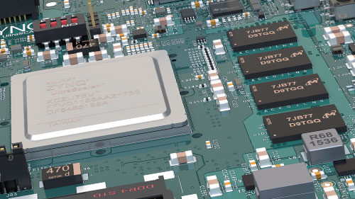
The defense manufacturer was developing a next‑generation embedded platform with high levels of integration and dense digital architecture. The complexity of this platform, combined with its use in demanding operational environments, made reliable test access a critical requirement.
These boards featured:
- High pin‑count FPGA/BGA devices
- Fine‑pitch high‑density connectors
- Large programmable logic components
- Dense multi‑layer architecture
All of which made traditional probing slow, unreliable, or impossible. Engineers needed a faster, more scalable way to debug and test both JTAG and non‑JTAG components.
The Turning Point
This leading defense manufacturer selected advanced boundary scan as its preferred platform for development, first article build, production, and field service, adopted both internally and by its manufacturing.
The engineering team quickly found that smarter structured testing provided a cost‑effective and highly intuitive way to get up and running fast, enabling engineers to move from setup to meaningful test coverage within hours rather than days.
Within hours, engineers achieved around 80% test coverage on complex digital circuitry-even on sections that were previously inaccessible.
Why It Works
Advanced boundary scan testing delivered a unified approach that worked across development, production, and support, removing much of the friction typically associated with complex board bring-up.
Key advantages:
- Reusable device‑centric tests that work across multiple boards and future projects
- Testing of JTAG and non‑JTAG devices through a high‑level structural test method scripting
- Rapid programming of flash and other devices from development through production
- Fast fault isolation in densely populated PCBAs
- Portable structural test scripts that can be reused across different designs, reducing engineering effort and improving long-term maintainability
Results
- ≈20% reduction in debug and test development time
- 80%+ digital coverage achieved rapidly
- Unified design‑for‑test strategy across development, first article build, production, and field service
- Reusable scripts enabling faster future projects
- Cost‑effective testing for boards containing large numbers of JTAG and non‑JTAG devices
The organisation also recognised that advanced boundary scan offered the speed, versatility, and cost‑effectiveness needed to support a unified design‑for‑test approach that could scale across the entire product lifecycle, from early development through production and ongoing support.
Call to Action
- See how these world leading defense companies are accelerating their design and testing using advanced boundary scan. Read the defense case studies here.
- Or explore more success stories, click here to see over 100 case studies.
- Now it is your turn to try advanced boundary scan for free with your own board and see how much faster you can debug, test, and program your designs.
Related Reading