Don’t Throw Away the Tests That Got Your Prototype Working

Image of CEO of XJTAG Simon Payne Simon Payne, CEO, XJTAG |  October 13, 2026 Subscribe to LinkedIn newsletter
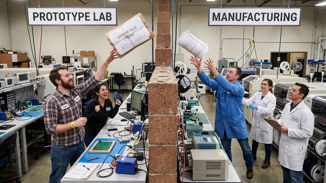
XJTAG Testing Times - Keeping prototype tests for manufacturing

The first prototype arrives and the engineering team begins the process of proving the hardware.

Connections are checked.

Memories are exercised.

Peripherals are tested.

Problems are found, understood and fixed.

Eventually, the board works.

And then something slightly strange can happen.

Much of the test capability that helped get it working is never used again.

Bring-Up Creates More Than a Working Board

During bring-up, engineers build up a significant amount of knowledge about the hardware.

They learn how to initialise devices.

They discover which signals need to be controlled.

They find ways of checking memories and peripherals.

They work out how to distinguish between a software problem and a hardware problem.

Sometimes this knowledge becomes a formal test.

Sometimes it is a small utility written by one engineer.

Sometimes it is little more than a sequence of commands, measurements or notes that helped prove a particular part of the board.

But whatever form it takes, it has value.

The question is:

What happens to it once the prototype works?

A Test Shouldn’t Necessarily Be Used Only Once

Some bring-up tests are naturally temporary.

But many aren’t.

If a test helped prove that an interface was correctly connected on the first prototype, there may be no reason why the same test cannot help verify that interface again later.

The purpose simply changes.

During bring-up, the question might be:

“Did we design this correctly?”

During production:

“Has this particular board been assembled correctly?”

During repair:

“Which part of this board is no longer behaving correctly?”

Different stages of the product lifecycle.

But often the same underlying hardware evidence is useful.

Turn Engineering Knowledge into Something Repeatable

There is an important difference between knowing how to test something and having a test that someone else can run.

If an engineer manually performs a sequence of checks during bring-up, that knowledge may disappear when the project moves on.

If the same procedure is documented and automated where practical, it becomes reusable.

That means the effort invested during development can continue providing value.

Instead of every new team starting again, the product carries some of its diagnostic knowledge with it.

Boundary Scan Is Particularly Well Suited to Reuse

Boundary Scan can be especially useful here because structural tests are based on the hardware and its connectivity rather than depending entirely on the final application software.

A test created to verify connections between devices during bring-up can potentially verify those same connections during manufacturing.

A test used to exercise a memory, peripheral or other accessible device may remain useful during fault diagnosis.

The reason for running the test changes.

The physical hardware being checked does not.

That gives structural tests the potential to move with the product from development into production and later support.

Don’t Lose the Tests at Handover

When a product moves from development into manufacturing, the handover typically includes things such as:

  • Schematics
  • PCB data
  • BOMs
  • Manufacturing information
  • Firmware
  • Programming files
  • Test specifications

It is worth asking whether the diagnostic capability developed during bring-up should be treated in exactly the same way.

Which tests proved particularly useful?

Which interfaces can be independently verified?

Which procedures helped isolate previous faults?

Which tools or scripts should be retained?

If that knowledge stays with one engineer rather than moving with the product, its value can easily be lost.

One Investment, Several Uses

The same test capability can potentially support:

  • Prototype bring-up — establishing confidence in the first hardware.
  • Design verification — proving that important areas of the PCB behave as intended.
  • Production — checking whether individual assemblies have been manufactured correctly.
  • Repair and rework — confirming whether a fault has been successfully corrected.
  • Failure analysis — narrowing down where to investigate a returned board.
  • Long-term support — providing engineers with diagnostic capability years after the original development team has moved on.

That starts to change the way we think about the cost of developing a test.

It isn’t necessarily an investment for one stage of the project.

It can be an investment in the product’s entire lifecycle.

Where XJTAG Fits

This is one reason an XJTAG project can become more than something used to bring up the first prototype.

Once the design information, device models and tests have been developed, that work can potentially be reused as the product moves into manufacturing, repair and support.

Rather than rebuilding the test strategy at every stage, the same underlying project can evolve with the hardware.

The value isn’t simply in running another test.

It is in preserving and reusing what the engineering team has already learned.

Closing Thought

Getting the first prototype working shouldn’t necessarily be the point at which your test investment ends.

It can be the point at which that investment starts becoming reusable.

The tests that help an engineer understand board number one may also help manufacturing verify board number 1,000—or help a service engineer understand a failure years later.

A good test isn’t just something you run.

It’s engineering knowledge you can reuse.


Board Design Tip of the Week

When your next prototype reaches the point where everyone agrees it is working, don’t immediately move on.

Ask: “Which of the tests and diagnostic procedures we’ve developed should follow this product into production and support?”

Capture them.

Document them.

Automate them where practical.

And consider keeping them under the same configuration control as the rest of the product.

The knowledge required to prove the first board works may be just as valuable when a board much later in the product’s lifecycle doesn’t.


Discover more about your board design with the Free XJTAG Layout Viewer.

To get started find out how the Free XJTAG Layout Viewer can help you see on your board:

Download your Free XJTAG Layout Viewer today
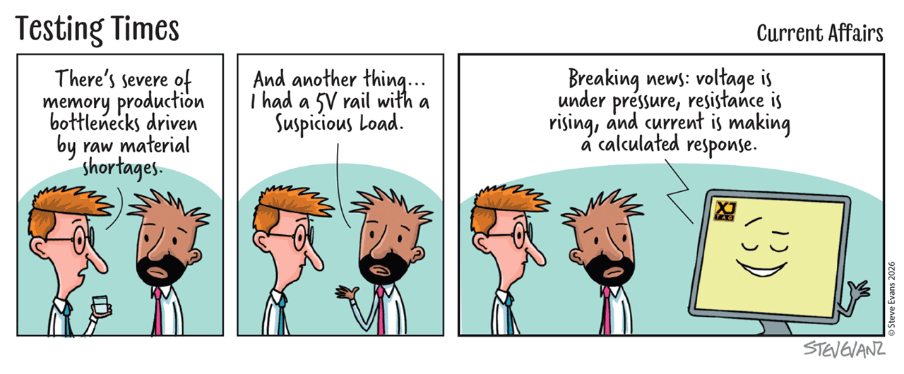

XJTAG Testing Times cartoon - Current affairs

Testing Times - PCB engineers in workshop, asking what JTAG is
Your Device Has JTAG. But Can You Actually Use It? Many engineers select an FPGA, processor or SoC and see JTAG support listed in the device specification. That sounds reassuring. The capability is there. But there is an important catch: If the PCB design doesn't provide practical access to that JTAG interface, much of the value has already been lost before the first board is built. And that can mean giving up access to one of the most useful diagnostic capabilities already built into the silicon. JTAG Is Easy to Overlook During Design When a new PCB is being developed, there is a lot competing for attention. DDR, PCIe, Ethernet, Clocks, Power, High-speed interfaces and Peripherals. Compared with those, JTAG can look relatively unimportant. It may be seen simply as something required to program an FPGA or connect a processor debugger. And if programming is going to happen through another mechanism, it can be tempting to think: “We don't really need JTAG on the finished board.” That decision may remove considerably more capability than expected. JTAG Is More Than a Programming Interface Programming and processor debug are probably the most familiar uses of JTAG. But, as we've explored throughout Testing Times, many modern semiconductor devices also contain Boundary Scan logic. That can give engineers access to the signals around the device independently of the application software. With the right board design, that access may help verify PCB connectivity, investigate memories and peripherals, exercise control signals and establish confidence in hardware before the application is even running. The semiconductor manufacturer has already provided much of this capability inside the device. The PCB designer decides whether it remains accessible. The Capability Is Already There This is an important point. Adding JTAG access doesn't mean adding an entirely new test technology to the design. For many devices, the hardware is already in the silicon. The design task is largely about making sensible provision for using it. That might mean routing the JTAG signals to a connector, test pads or another accessible interface. On a more complex board, it may mean considering how several devices should be arranged into one or more JTAG chains. The incremental design effort can be small. The potential value later can be considerable. Think Beyond the First Prototype The obvious time to value JTAG access is during bring-up. If the processor doesn't boot or the FPGA application isn't ready, JTAG and Boundary Scan may provide another route into the hardware. But its usefulness doesn't necessarily stop once the prototype works. The same access can potentially support: Programming and configuration Development and debug Structural testing Manufacturing test Failure analysis Repair and rework Long-term product support A connector that seems unnecessary during schematic capture may become extremely useful several years later when someone has to diagnose a board that no longer behaves as expected. Don't Just Put the JTAG Pins on the Schematic Providing JTAG access requires a little more thought than simply connecting TCK, TMS, TDI and TDO. During design, it is worth asking: Where will the interface actually be accessed? Are all the devices you may want to reach included in a usable chain? What happens if one device is unpowered or not fitted? Are suitable pull resistors and termination options provided? Can relevant mode or configuration pins be placed into the required state? Would several JTAG chains provide better flexibility on a complex system? Will JTAG still be accessible on the production board? These are relatively easy questions to answer before layout. They become much harder to solve once assembled PCBs are sitting on the bench. What Happens If You Don't Route It Out? Perhaps nothing. The board may work perfectly. The firmware may work first time. Production may run smoothly. But if something does go wrong, one useful source of visibility is no longer available. A processor that won't boot becomes harder to investigate. An FPGA board with incomplete firmware may provide fewer diagnostic options. A production failure may need to be approached entirely through functional testing or physical probing. The problem isn't that the product suddenly cannot be tested. It is that an existing diagnostic option has been designed away. Closing Thought Seeing “JTAG supported” in the device datasheet isn't enough. The semiconductor manufacturer has provided the capability. The PCB designer decides whether anyone will actually be able to use it. Routing JTAG access may occupy only a very small part of the schematic. But it can provide useful visibility throughout the life of the product. And the easiest time to preserve that capability is before the PCB exists. Board Design Tip of the Week If you're providing JTAG access, build in a little flexibility rather than designing only for the configuration you expect to use today. Consider providing footprints for appropriate JTAG pull resistors and termination components, even if some are initially left unpopulated. Where device configuration or mode pins can affect JTAG operation, consider providing resistor options that allow those states to be changed if necessary. And if a permanent JTAG connector isn't desirable on the production PCB, consider retaining accessible test pads or another practical connection method. Those small provisions cost very little at the design stage, but they can give engineers considerably more options during bring-up, test and fault diagnosis later. Could JTAG boundary scan help you test your next design? Discover how boundary scan can help you improve test coverage, diagnose faults faster and simplify board testing: Find out more about JTAG boundary scan and how it can help you. Discover more about your board design with the XJTAG Layout Viewer. To get started find out how the XJTAG Layout Viewer can help you see on your board: Download your free XJTAG Layout Viewer today
Testing Times - PCB engineers in workshop, testing before firmware
Can You Test a Board Before the Firmware Exists? We were recently asked a very practical question: “Can you test our board using Boundary Scan? The firmware isn’t available yet.” The answer is yes, and this is exactly the kind of situation where Boundary Scan can provide real value. When the first assembled PCBs arrive, hardware engineers want to start establishing confidence in them immediately. Waiting for firmware before meaningful hardware testing can begin creates an unnecessary dependency between two development activities that are often progressing in parallel. The Hardware Often Arrives Before the Firmware This is a familiar situation on many development projects. The first assembled PCBs arrive. The hardware team wants to begin bring-up. But perhaps: The processor firmware is still under development The FPGA image is not yet available Device drivers have not been written The operating system is not running None of this necessarily indicates a problem with the project. Hardware and software development simply progress at different rates. The important question is whether hardware testing has to wait. Boundary Scan Doesn't Depend on Your Application One of the key advantages of Boundary Scan is that the test capability is built into the semiconductor devices themselves. It operates independently of the application software or FPGA design. So the processor does not need to have booted and the FPGA does not need to be configured with the product design before useful structural testing can begin. Boundary Scan can instead be used to gain access to PCB signals through the dedicated test logic already present in suitable devices. That access can help engineers verify things such as: PCB interconnections Address, data and control buses Connections to memories Connections to peripherals Resets, enables and other control signals Accessible interfaces and discrete circuitry The emphasis is primarily on establishing confidence in the connections between the devices and the PCB. Those connections can also be used to exercise part of a non-JTAG device's functionality, providing additional evidence that the surrounding circuitry is behaving correctly. Why That Matters During Bring-Up Suppose the firmware eventually arrives and a memory interface doesn't work. There are now several possibilities. Is there a firmware problem? Is the memory being initialised incorrectly? Is the FPGA or processor configuration wrong? Or is there a physical problem with one of the PCB connections? If structural tests have already established confidence in the relevant hardware, one major area of uncertainty has already been reduced. Instead of the hardware and firmware teams having to work out whose area contains the problem, they have independent evidence to help narrow the investigation. That can make bring-up considerably more systematic. Hardware and Firmware Can Progress in Parallel This is perhaps the broader benefit. Boundary Scan can help decouple initial hardware validation from firmware availability. While the software team continues developing the application, the hardware team can begin verifying accessible areas of the PCB. Then, when the firmware is ready, it starts from a stronger position. Some of the underlying hardware has already been independently checked. That does not remove the need for functional testing. It means functional testing begins with greater confidence in the hardware underneath it. It Helps the Firmware Team Too Firmware engineers are often among the first people to expose hardware problems because their software begins exercising interfaces that may never previously have been used. If a peripheral fails to respond, they can spend considerable time investigating code before discovering that the cause is actually a PCB connectivity problem, an incorrectly fitted component or another hardware issue. Providing the firmware team with boards that have already passed useful structural tests gives them a much better starting point. They can concentrate on developing and debugging the software without automatically becoming the first stage of hardware diagnosis. Start Building Confidence Earlier Functional testing usually needs enough of the system to be operational for the application to run. Boundary Scan works differently. It uses dedicated test logic within the semiconductor devices to provide access to the PCB independently of the application. That means useful hardware testing can begin much earlier in the development process. And when hardware and software teams are both working towards the same deadline, removing unnecessary dependencies between them can be extremely valuable. Closing Thought The question we were asked was: “Can you test the board even though the firmware isn't ready?” Yes. But perhaps the more useful question is: “Why wait for firmware before starting to build confidence in the hardware?” Hardware and firmware development often happen in parallel. The test strategy can too. Boundary Scan provides a way to start checking the PCB earlier, establish confidence in accessible areas of the hardware and reduce uncertainty before the application ever runs. Board Design Tip of the Week When planning a new design, ask what you could verify if no application software were available at all. Can important resets and enables be controlled? Can key interfaces and memory connections be accessed? Can critical signals be driven and observed? Is the JTAG chain readily accessible? Thinking about those questions during the design stage can give the hardware team useful diagnostic capability from the moment the first assembled PCB arrives — rather than from the moment the firmware does. Could boundary scan help you test your next design? Discover how boundary scan can help you improve test coverage, diagnose faults faster and simplify board testing: Find out how XJTAG can help you. Discover more about your board design with the Free XJTAG Layout Viewer. To get started find out how the Free XJTAG Layout Viewer can help you see on your board: Download your Free XJTAG Layout Viewer today
XJTAG Testing Times - PCB engineers in workshop
“It’s Only a Small Board Change…” What Could Possibly Go Wrong? We recently spoke to an engineer about a new revision of an existing PCB. The message was: “It’s only an iterative change.” The implication was understandable: the design changes are small, so the additional test work should also be small. And they may be absolutely right. But it raises an important question: How do you know? A small PCB revision does not automatically mean a small test impact. How Much Test Work Does a Small PCB Revision Really Create? The answer depends less on how many things changed and more on what those changes affect. A reset signal may have moved. A buffer may have been added. A memory device may have been replaced. A previously unused FPGA pin may now be connected. A power rail or enable sequence may have changed. Each change may be small on the schematic, but if an existing test depends on it, the impact can be much greater. Every test makes assumptions about the hardware: which devices are fitted, how signals are connected, what can be controlled and observed, and how devices behave during test. Change one of those assumptions and the existing test may need to change too. What If the Change Is at the Centre of the Board? Now consider replacing the FPGA or processor at the heart of the design. Perhaps the new device performs essentially the same function and most of the surrounding circuitry is unchanged. It may look like a straightforward substitution. But that device may interact with a significant proportion of the board and therefore affect many existing tests. For teams using Boundary Scan, there is another important consideration: Is the BSDL file correct for the exact device and package now fitted? Boundary Scan software relies on the BSDL file to describe the device's pins, Boundary Scan cells, instructions and test capability. So a change that appears on the design change list as: “FPGA changed from A to B” could potentially affect considerably more of the existing test strategy than the change list initially suggests. This is why test effort isn't proportional to the number of changes. It depends on how central those changes are to the tests already developed. Regression Testing Isn't Just for Software Software engineers are familiar with regression testing. A small code change doesn't mean rewriting the entire application, but it does mean understanding what else could have been affected. PCB test deserves the same approach. For every revision, ask: What changed? Which existing tests depend on it? Which assumptions are still valid? Which tests can remain unchanged? Which tests need modifying? Is any additional test coverage required? The objective isn't to assume everything has changed. It's to avoid assuming nothing has. Reuse Should Still Be the Goal Last week, we looked at the value of reusing tests developed during bring-up through production, repair and support. A new board revision shouldn't change that principle. Good reusable tests should make iterative development easier. The aim is to preserve everything that remains valid and concentrate engineering effort only on the tests affected by the new design. Reuse the test — but validate the assumptions behind it. That is far more efficient than designing a complete test strategy again for every PCB revision. Closing Thought “It’s only an iterative change” may be completely true. And the additional test-development work may genuinely be trivial. But that should be the conclusion of an impact review, not the assumption at the start of one. When the next PCB revision is released, ask: What changed? Which of our existing tests depend on those changes? Are the assumptions behind those tests still valid? Then preserve everything that still works. The objective isn't to design a complete test from scratch. It's to know which tests need changing — and why. Board Design Tip of the Week When documenting your next PCB revision, add one more item to the change list: Test impact. For each design change, consider whether it affects: Component functionality or pinout Signal routing or connectivity Resets, enables or mode settings Power rails or sequencing Interfaces and control signals Physical test access Programming or configuration Existing test assumptions And if Boundary Scan forms part of your test strategy, also check whether the change affects the BSDL/device model or JTAG architecture. A short review at this stage can prevent a “small change” from becoming an unexpected test-development problem when the revised boards arrive. Discover more about your board design with the Free XJTAG Layout Viewer. To get started find out how the Free XJTAG Layout Viewer can help you see on your board: Download your Free XJTAG Layout Viewer today