Find Out How You Can Bring Complex Processor and FPGA Boards to Life Faster
 Simon Payne, CEO, XJTAG
|
Subscribe to LinkedIn newsletter

Intro
If you’ve worked on building embedded systems, you’ve likely faced this problem before. As boards built around processors, FPGAs, and System‑on‑Chip (SoC) devices become more powerful and more densely packed, test access disappears just when you need confidence most. With pressure to move quickly from prototype to production, traditional testing methods often fail to give you the visibility required to ensure reliability.
That’s why more engineers are adopting structured testing approaches that reveal hardware connectivity long before firmware is available, reducing risk and accelerating development.
The Challenge
You have a board on the bench. Power rails are good. Clocks are present. But the system won’t boot.
No firmware output. No LEDs. No clear indication of what’s wrong.
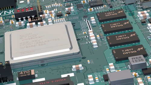
For designs built around CPUs, FPGAs, and SoCs, this scenario is all too common. These boards typically include:
- High‑pin‑count processors, FPGAs, and SoCs
- High‑speed memories and complex bus interfaces
- Dense BGA, CSP, or WLP packages with thousands of hidden connections
Without visibility into these high‑density interconnects, engineers are forced to guess. Is the device fully soldered? Are memory interfaces connected correctly? Are critical peripherals even reachable? Each unanswered question costs hours, delays schedules, and increases development risk.
The Turning Point
Structured boundary scan testing gives you a way to answer these questions quickly and safely.
By using the JTAG interface already present on most processors, FPGAs, and SoCs, you can verify board-level connectivity and device-to-device links without relying on firmware or physical probing.
With this approach, you can:
- Detect shorts, opens, and stuck‑at faults early
- Verify solder joints and interconnects beneath BGAs and on fine‑pitch devices
- Confirm memory buses and peripheral connections before first boot
- Begin fault isolation immediately, rather than waiting on software
This shifts board bring‑up from trial‑and‑error to structured validation.
Why It Works
Boundary scan operates at low speed and focuses on static connectivity, which is exactly why it is so effective for complex embedded designs.
Too often, teams assume functional tests alone are enough to confirm solder quality and I/O connectivity, particularly on high‑speed interfaces and memory devices. In practice, this assumption introduces risk.
There are two fundamental limitations with relying solely on functional testing:
- Undetected faults – Cold solder joints, marginal opens, and partial connections can appear to function correctly at speed due to capacitance effects. These hidden issues often degrade over time, leading to intermittent or early‑life failures that are extremely costly to diagnose once systems are deployed.
- Limited fault insight – When functional tests do fail, they rarely indicate what is wrong or where the fault is located. Engineers are left to spend significant time developing additional tests or probing blindly, slowing fault isolation and increasing debug cost.
Structured boundary scan addresses these gaps by validating physical connectivity directly, before firmware or high‑speed operation can mask underlying issues.
Key advantages:
- Deep visibility into device pins and interconnects where probes cannot reach
- Early fault detection before firmware or functional tests are available
- Clear diagnostics, identifying what failed and where
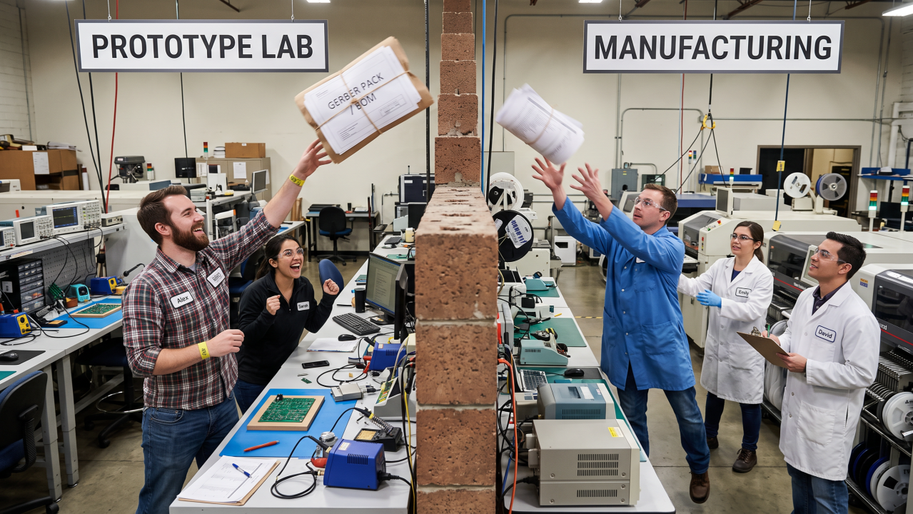
- Reusable test assets that scale from prototype to production
- Consistent workflows across development, manufacturing, and in‑field support
Rather than replacing functional testing, structured testing complements it, closing the gap between hardware assembly and software validation.
Results
Teams using structured testing on processor‑ and FPGA‑based boards report:
- Faster board bring‑up and earlier confidence in hardware integrity
- Reduced debug time on non‑booting systems
- Fewer surprises during production ramp‑up
- Improved test coverage on dense, high‑pin‑count devices
- Shorter time‑to‑market for complex embedded products
By validating hardware earlier, fixes are applied when they are fastest and least expensive.
Take the Next Step
- Discover how you can validate CPU, FPGA, and SoC‑based designs faster using structured testing.
- Explore more than 100 real‑world success stories. View case studies.
- Learn how improved hardware visibility can reduce risk on your next design. Start your free evaluation on your own board today.
Related Reading