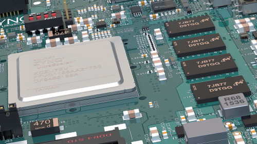
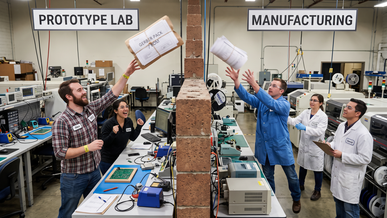
Why FPGA Reference Designs Don’t Fail – But Real Boards Do
 Simon Payne, CEO, XJTAG
|
Subscribe to LinkedIn newsletter

FPGA reference designs are reassuring.
They power up. They configure cleanly. Interfaces behave as documented. Examples run exactly as expected.
That predictability is not accidental. Reference designs are carefully engineered, validated, and iterated by teams whose only job is to make them work reliably.
And that’s precisely why they can create a false sense of security.
The Hidden Assumption in Bring-Up
When transitioning from a development board or reference platform to a custom PCB, an assumption often travels with the design:
“If it worked there, it should work here.”
Logically, that makes sense.
But physically, the situation has changed.
Different layout. Different power architecture. Different impedance control. Different assembly environment. Different tolerances.
The FPGA may be the same part number — but the system around it is not.
What Reference Designs Quietly Protect You From
Reference platforms shield engineers from a range of subtle issues:
- Marginal power sequencing
- Layout-induced noise
- Skew between control signals
- Assembly variability
- Manufacturing defects
When those protections disappear in a custom design, problems that never appeared on the reference board suddenly surface.
Not necessarily because the firmware or FPGA design is wrong — but because the environment is different.
When “It Worked on the Dev Board” Becomes a Trap
One of the most common early bring-up phrases is:
“But it worked on the dev board.”
That statement is emotionally understandable — but technically incomplete.
The development board proved:
- The silicon can perform the function
- The FPGA configuration is viable
- The architecture makes sense
It did not prove:
- Your board routing is correct
- Your assembly is flawless
- Your board-level connectivity matches intent
Those are separate proofs.
Structural Confidence vs Functional Confidence
Reference designs provide functional confidence.
Custom boards require structural confidence.
Until structural confidence is established — meaning power, connectivity, configuration paths, and access are verified — functional debugging is built on assumptions.
This is why experienced teams separate the phases:
- Prove the structure.
- Then prove the behaviour.
Not the other way around.
Closing Thought
Reference designs are invaluable. They accelerate development, reduce architectural uncertainty, and shorten time-to-first-light.
But they do not eliminate the need to prove that your own board is electrically what you believe it to be.
The fastest bring-up teams don’t assume transferability. They establish proof at each new stage.
FPGA Board-Level Tip of the Week
Design custom boards so critical FPGA access paths can be verified independently of application firmware.
When moving from a reference design to a custom board, ensure that essential access and configuration paths can be tested without relying on the full system being operational.
Why it matters
- Prevents firmware issues from masking hardware faults
- Allows early isolation of structural problems
- Reduces the risk of misattributing connectivity issues to logic
What to watch out for
- Mode pins or reset conditions that disable access unintentionally
- Clock dependencies that prevent simple structural checks
- Watchdogs that can’t be disabled without functioning firmware
- Incorrect routing or termination of JTAG signals
Designs that assume the FPGA must be fully configured before any validation can occur. Structural validation should not depend on full system functionality.
Related Reading