XJAccelerator SODIMM Module
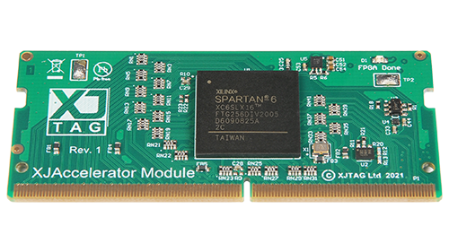
XJAccelerator SODIMM is a multi-purpose FPGA module in a 260-pin SODIMM form factor. It is designed to be integrated into a test fixture assembly to extend test coverage and to facilitate and accelerate programming functions.
Key Benefits
Simplifies the test fixture design process and reduces development time
Increases UUT test coverage by providing additional connectivity
Easy integration with XJTAG test systems
Fast flash programming (XJFlash) compatible
Features
- Reconfigurable
- FPGA module
- Supports SPI, I2C, ICSP, SWD, and other protocols
- NOR flash programming, including Quad-SPI and Octal-SPI devices
- 260-pin SODIMM interface
- Flexible I/O voltage levels (four banks)
- 161 single-ended I/O or up to 78 differential pairs (or a mix of both)
Boundary scan enabled test fixture
Based on a Xilinx® Spartan®-6 FPGA, the XJAccelerator SODIMM module is principally designed to maximise a test fixture’s test coverage by providing a JTAG device that adds boundary scan capability. It allows a large amount of UUT I/O to be tested, and multiple modules can be daisy chained to provide additional capacity.
Test fixture control
The boundary scan capabilities of any unused I/O pins can be used to control the test fixture and to provide fast hardware-based monitoring and responses. For example, this could allow supply rail monitoring and rapid over-current shutdown, with profiled thresholds to prevent in-rush currents causing false-triggering.
Accelerated programming
This versatile platform can also provide accelerated programming of NOR flash devices provided it is given access to all the required signals. In this mode, the FPGA is configured with XJFlash, and data is streamed into the module over JTAG. Flash memories with any of the interface protocols supported by XJFlash can be programmed, and the module supports the option of concurrent programming of multiple devices to reduce overall programming times.
The FPGA can be configured through its JTAG port as part of a standard XJTAG project or from the module’s PROM.
Flexibility and ease of use
The module uses a standard SODIMM connector for easy connection to a test fixture board.
Each of the FPGA’s four I/O banks is powered independently from supplies external to the module (1.1 to 3.3 V). This provides versatile handling of multiple voltage domains.
The XJAccelerator module can be connected to a JTAG controller in various configurations, allowing easy integration into a wide range of projects. It can be connected to a dedicated TAP on a JTAG controller or added in series with the JTAG chain of a UUT.
JTAG multiplexer
The FPGA can be configured as a JTAG multiplexer (scan bridge). Chains can be routed directly to the module to minimise cable lengths, helping to maintain the signal integrity of JTAG signals.
Product code:
ACS-0010. Please contact your local distributor for a quote.
Compatible with:
| XJLink-PF40 | XJLink2 | PXI-XJLink2 | XJQuad | Other |
| N/A | N/A | N/A | N/A | Fits into SODIMM socket on UUT |