Find Out How a Leading Electronic Design Company Shaves Weeks Off Debug and Testing
 Simon Payne, CEO, XJTAG
|
Subscribe to LinkedIn newsletter

When deadlines are tight and designs are complex, every hour saved in debugging counts. That’s exactly what one advanced RF technology product developer achieved a faster time to market by adopting smart testing to speed up development, improve coverage, and streamline production.
The Challenge
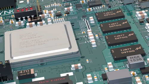
The company develops cutting-edge spectral analysis products used for real-time spectrum monitoring across multiple industry sectors. Their advanced system, built around a Xilinx FPGA, surveys a wide frequency range to map and manage radio spectrum usage.
But behind the innovation came complexity. Each of their advanced RF system boards featured a high pin-count FPGA, a nightmare for traditional testing. Probing those densely packed BGAs wasn’t just time-consuming; it was next to impossible.
The Turning Point
That’s when the company turned to smart testing. The switch changed everything.
Their engineers could test the Xilinx FPGA (a JTAG enabled device) and extend the testing to non-JTAG devices on their board by using advanced boundary scan, achieving over 80% device coverage across the their boards, all without complex test fixtures. Tests that once took weeks to validate could now be completed in a fraction of the time.
Why It Works
Boundary-scan testing, defined by IEEE 1149.x, allows engineers to validate connections and functionality without physically probing every device pin. This can then be taken further with an intuitive development environment, making it easier to write, reuse, and share tests across multiple boards and projects.
By testing from the device’s perspective, the company could reuse test scripts between modules, saving engineering time and ensuring consistency. And by visualising results and isolating faults development became faster than ever.
The Results
- Weeks of debugging reduced to days
- 80%+ device coverage achieved via advanced boundary scan
- Reusable tests across multiple products and projects
- Simplified production testing through reusable test harnesses
The company now uses advanced boundary scan across the entire product lifecycle from design and development to contract manufacturing, ensuring every board leaving production meets the highest standard of reliability.
See how this world leading company is accelerating their design and testing using advanced boundary scan. Read the case study here.
Or explore more success stories, click here to see over 100 case studies.
Is it time to try XJTAG for free with your own board and see how much faster you can debug, test, and program your designs?
Related Reading