Why Understanding the Board Matters More Than Ever
 Simon Payne, CEO, XJTAG
|
Subscribe to LinkedIn newsletter

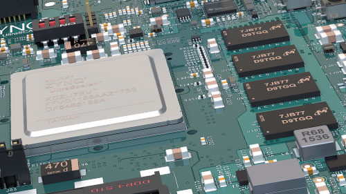
Today’s electronics are incredibly powerful. As boards become denser and more complex, one challenge continues to grow quietly in the background:
simply understanding what is connected to what
During bring-up, debug, and test, engineers are constantly asking questions like:
- Where does this signal actually go?
- Which devices are connected to this net?
- Is this behaviour expected?
- What part of the board has already been proven?
The answers already exist inside the design data.
The problem is often visibility.
The Growing Visibility Problem
As electronic systems evolve, so does board complexity:
- more layers
- more BGAs
- more high-speed interfaces
- more hidden connectivity
And while schematics remain essential, tracing signals manually across dense layouts can quickly become time-consuming and frustrating.
Particularly when:
- debugging hardware issues
- investigating manufacturing faults
- validating connectivity
- or simply trying to understand an unfamiliar design
Seeing the Board Changes the Process
One thing we’ve seen repeatedly over the years is this:
The faster engineers can visualise the board, the faster they can:
- understand problems
- isolate faults
- verify assumptions
- and move development forward
Because often, the bottleneck isn’t solving the issue itself.
It’s understanding the hardware clearly enough to know where to focus.
Introducing the Free XJTAG Layout Viewer
To help make this easier, we created the XJTAG Layout Viewer, a free standalone tool for exploring PCB layouts using ODB++ design data.
It allows engineers to:
- Search and highlight nets, pins, and devices
- Visualise signal connectivity clearly
- Navigate dense layouts quickly
- Trace connections across the PCB
- Understand board structure more intuitively
The goal is simple:
Reduce the time spent trying to understand the board
Particularly Useful For
The Layout Viewer is especially valuable when working with:
- BGA-based systems
- complex multilayer boards
- manufacturing debug
- board bring-up
- fault investigation
- unfamiliar hardware designs
Whether you’re validating a new prototype, investigating a failure, or simply trying to understand how a system is connected, being able to visualise the board directly can dramatically improve workflow efficiency.
More Than Just Viewing Layouts
One of the interesting things we’ve observed is that once engineers can clearly see the hardware, many other processes become easier:
- debugging becomes more focused
- communication improves between teams
- manufacturing issues are easier to isolate
- confidence in the hardware increases
In many cases, simply improving visibility removes a surprising amount of friction from development.
Closing Thought
In complex electronic systems, uncertainty often comes from not being able to clearly see what’s happening on the board.
The faster that visibility is established, the faster engineers can move from:
- confusion
- to understanding
- to confidence
And sometimes, that starts with something very simple:
being able to see the connections clearly.
Related Reading