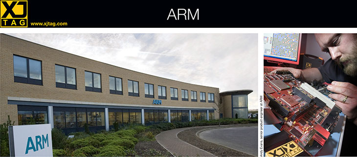
TTPCom selects XJTAG system for debug and test of BGAs on wireless development platform

  • The XJTAG boundary scan system enables TTPCom to diagnose and debug faults on its 2G/3G development platform, which contains multiple ball grid array (BGA) devices with over 9,500 connections
  • XJTAG’s unparalleled speed and accuracy of test and debug has enabled TTPCom to shave days/weeks off the development phase of its wireless platform
  • XJTAG selected ahead of competition due to the speed of fault diagnosis, the accuracy of debug, ease-of-use, reusability of scripts, and the quality of technical support

CAMBRIDGE, England, March 30, 2006 – TTPCom, a world-leading independent supplier of software and silicon intellectual property (IP) for digital wireless terminals, has selected the XJTAG development system as its boundary scan test solution. The XJTAG system enables engineers at TTPCom’s headquarters in Cambridge, England, to diagnose and debug its wireless development platforms, which contain a plethora of ball grid array (BGA) devices and over 9,500 connections. XJTAG is also used by TTPCom’s contract manufacturing partners.

TTPCom selected the XJTAG system predominantly to test and debug the numerous JTAG devices on its development boards. These include five 1152-pin Xilinx field programmable gate arrays (FPGAs), an ARM9 microprocessor control unit (MCU), a high-speed digital signal processor (DSP), a clock controller and a number of other programmable logic devices (PLDs).

“The XJTAG system is a perfect fit for our development requirements as it enables us to read and write to all of the device pins in the JTAG chain using the XJAnalyser circuit visualisation tool,” said Andrew Evans, design engineer within TTPCom’s silicon hardware group. “With XJTAG, we can view the pin states on screen to quickly locate bridges, breaks, poor joints or incorrect connections, and then isolate any faulty device and rework or reflow it to rectify the problem.”

TTPCom develops designs for the full range of technologies required to deliver a successful cellular handset from antenna to applications. The company delivers tried and tested intellectual property for all components, enabling manufacturers to build working models quickly and allowing them to concentrate on value adding activities that differentiate their products. TTPCom is actively engaged at all stages of handset development through its worldwide collaboration with leading silicon manufacturers, software vendors and handset manufacturers.

TTPCom’s dual mode (2G and 3G) pre-silicon development board is a mobile phone reference platform with extensive development and debug capabilities built-in. It is used by TTPCom to develop and warrant intellectual property (IP), to demonstrate operations and assist with conformance testing. The development platform is also used by customers for developing their own silicon and software.

“It’s important that we get these complex development boards up and running quickly and verify that each one is built according to the schematics as they are used extensively across the business and cost many thousands of dollars,” says Jonathan Healy, design engineer at TTPCom. “XJTAG has exceeded our expectations. Its unparalleled speed, accuracy and ease-of-use have enabled us to shave days, if not weeks, off the development phase of our wireless reference platforms – important factors in the mobile phone industry where time-to-market is so critical.”

The XJTAG boundary scan development system meets the growing market need for a cost-effective solution for testing printed circuit boards populated with JTAG devices such as BGA and chip scale devices, which cannot be tested by traditional methods such as flying probes, logic analyzers, oscilloscopes and X-ray systems.

“XJTAG is designed by engineers for engineers and represents a major advance in testing/debugging techniques,” added Andrew Evans. “We looked at other boundary scan systems but opted for XJTAG due to the speed of fault diagnosis, reusability of scripts, and because their engineers were prepared to go that extra mile. In addition, because XJTAG abstracts engineers from the level of the JTAG bitstream, it makes JTAG easier and more intuitive to use.”

The XJTAG Development System is designed to cut the cost and shorten the development cycle of electronic products and provides a unique solution that can test JTAG as well as non-JTAG devices. XJTAG can test a high proportion of a circuit including BGA and chip scale devices, SDRAMs, Ethernet controllers, video interfaces, Flash memories, FPGAs, microprocessors and many other devices. XJTAG also enables In-System Programming of FPGAs, CPLDs (Complex Programmable Logic Devices) and Flash memories.

For more information about the XJTAG Development System, please contact XJTAG, St John’s Innovation Centre, Cowley Road, Cambridge, CB4 0DS, UK. Telephone +44 (0) 1223 223007, fax +44 (0) 1223 223009 or email enquiries@xjtag.com. Alternatively visit www.xjtag.com.

About TTPCom (www.ttpcom.com)

With 10 offices and development centres around the world, TTPCom Ltd. is the principal operating subsidiary of TTP Communications plc (LSE: TTC). The company develops intellectual property used in the design and manufacture of wireless communication terminals. TTPCom licenses its technology to leading semiconductor and terminal manufacturers worldwide, including Analog Devices, Intel, LG, NEC, Renesas, Sharp and Siemens.

TTPCom has established a world leading position with its GPRS, EDGE and 3G protocol software; offers rapid customisation of handsets through the AJAR Platform applications framework; and develops both radio and baseband cellular engines through its Macro products. More than 150 million devices using TTPCom technology have been shipped worldwide. More information can be found on TTPCom’s website at: www.ttpcom.com.

About XJTAG (www.xjtag.com)

XJTAG is a specialist design and test tool developer. Its JTAG (Joint Test Action Group) development system offers a competitive solution for designers and developers of electronic circuits. Utilising XJTAG allows the circuit development and prototyping process to be shortened significantly by facilitating early test development, early design validation, fast development of functional tests and test re-use across circuits that use the same devices. The company is based in the UK at St John’s Innovation Centre, Cowley Road, Cambridge. XJTAG is part of the Cambridge Technology Group (www.cambridgetechgroup.com).

What is JTAG?

Advances in silicon design, such as increasing device density and, more recently, ball grid array (BGA) and chip scale packaging, have reduced the efficacy of traditional electronic circuit testing methods. In order to overcome these problems and others; some of the world’s leading silicon manufacturers combined to form the Joint Test Action Group (JTAG). The findings of this group were used as the basis for the Institute of Electrical and Electronic Engineers (IEEE) standard 1149.1: Standard Test Access Port and Boundary Scan Architecture and subsequently the standard became known as JTAG.

Images (click for high resolution versions)

Jonathan Healy, design engineer at TTPCom, using XJTAG

Ready to get started? Try XJTAG

computer

See XJTAG in action.

Our experts will be happy to show you how the XJTAG tools can help you diagnose faults on your board as well as cutting test development and repair time.

Ask for a Demo

contact us icon

Questions? Contact us!

We're here to help.
Send us a message and one of our test specialists will get back to you shortly.

Contact us

workstation

Get a free test setup.

Evaluate the XJTAG system with full functionality for 30 days and get the first test project set up for your board – for free. No obligation to purchase.

Get started now

Join world leading companies using XJTAG Boundary Scan