Technical Guide to JTAG
Introduction
This document provides you with interesting background information about the technology that underpins XJTAG. However, you do not need to know this in order to use XJTAG’s products, because XJTAG testing operates at a higher level which does not require knowledge of the detailed workings of JTAG.
Advances in silicon design such as increasing device density and, more recently, BGA packaging have reduced the efficacy of traditional testing methods.
In order to overcome these problems, some of the world’s leading silicon manufacturers combined to form the Joint Test Action Group. The findings and recommendations of this group were used as the basis for the Institute of Electrical and Electronic Engineers (IEEE) standard 1149.1: Standard Test Access Port and Boundary Scan Architecture. This standard has retained its link to the group and is commonly known by the acronym JTAG.
Boundary Scan
The main advantage offered by utilising boundary scan technology is the ability to set and read the values on pins without direct physical access.
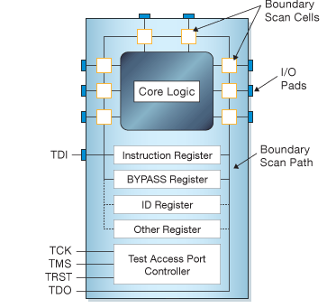
Figure 1 – Schematic Diagram of a JTAG enabled device
The process of boundary scan can be most easily understood with reference to the schematic diagram shown in figure 1.
All the signals between the device’s core logic and the pins are intercepted by a serial scan path known as the Boundary Scan Register (BSR) which consists of a number of boundary scan ‘cells’. In normal operation these boundary scan cells are invisible. However, in test mode the cells can be used to set and/or read values from the device pins (or in ‘internal’ mode from values of the core logic.) Not all boundary scan cells are the same – there are 10 types of cell in the 1149.1 standards, though manufacturers can define non-standard cell types to match the actual hardware functionality of their device if they wish.
Interface Signals
The JTAG interface, collectively known as a Test Access Port, or TAP, uses the following signals to support the operation of boundary scan.
- TCK (Test Clock) – this signal synchronizes the internal state machine operations.
- TMS (Test Mode Select) – this signal is sampled at the rising edge of TCK to determine the next state.
- TDI (Test Data In) – this signal represents the data shifted into the device’s test or programming logic. It is sampled at the rising edge of TCK when the internal state machine is in the correct state.
- TDO (Test Data Out) – this signal represents the data shifted out of the device’s test or programming logic and is valid on the falling edge of TCK when the internal state machine is in the correct state.
- TRST (Test Reset) – this is an optional pin which, when available, can reset the TAP controller’s state machine.
Registers
There are two types of registers associated with boundary scan. Each compliant device has one instruction register and two or more data registers.
Instruction Register – the instruction register holds the current instruction. Its content is used by the TAP controller to decide what to do with signals that are received. Most commonly, the content of the instruction register will define to which of the data registers signals should be passed.
Data Registers – there are three primary data registers, the Boundary Scan Register (BSR), the BYPASS register and the IDCODES register. Other data registers may be present, but they are not required as part of the JTAG standard.
- BSR – this is the main testing data register. It is used to move data to and from the I/O pins of a device.
- BYPASS – this is a single-bit register that passes information from TDI to TDO. It allows other devices in a circuit to be tested with minimal overhead.
- IDCODES – this register contains the ID code and revision number for the device. This information allows the device to be linked to its Boundary Scan Description Language (BSDL) file. The file contains details of the Boundary Scan configuration for the device.
Test Access Port (TAP) Controller
The TAP controller, a state machine whose transitions are controlled by the TMS signal, controls the behaviour of the JTAG system. Figure 2, below, shows the state-transition diagram.
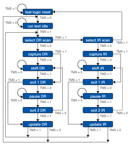
Figure 2 – TAP State machine
All states have two exits, so all transitions can be controlled by the single TMS signal sampled on TCK. The two main paths allow for setting or retrieving information from either a data register or the instruction register of the device. The data register operated on (e.g. BSR, IDCODES, BYPASS) depends on the value loaded into the instruction register.
For more detail on each state, refer to the IEEE 1149.1 Standard JTAG document.
Boundary Scan Instructions
The IEEE 1149.1 standard defines a set of instructions that must be available for a device to be considered compliant. These instructions are:
- BYPASS – this instruction causes the TDI and TDO lines to be connected via a single-bit pass-through register (the BYPASS register). This instruction allows the testing of other devices in the JTAG chain without any unnecessary overhead.
- EXTEST – this instruction causes the TDI and TDO to be connected to the Boundary Scan Register (BSR). The device’s pin states are sampled with the ‘capture dr’ JTAG state and new values are shifted into the BSR with the ‘shift dr’ state; these values are then applied to the pins of the device using the ‘update dr’ state.
- SAMPLE/PRELOAD – this instruction causes the TDI and TDO to be connected to the BSR. However, the device is left in its normal functional mode. During this instruction, the BSR can be accessed by a data scan operation to take a sample of the functional data entering and leaving the device. The instruction is also used to preload test data into the BSR prior to loading an EXTEST instruction.
Other commonly available instructions include:
- IDCODE – this instruction causes the TDI and TDO to be connected to the IDCODE register.
- INTEST – this instruction causes the TDI and TDO lines to be connected to the Boundary Scan Register (BSR). While the EXTEST instruction allows the user to set and read pin states, the INTEST instruction relates to the core-logic signals of a device.
Obtaining the IEEE 1149.1 Standard
The IEEE 1149.1 Standard JTAG specification is available directly from IEEE: