JTAG Testing with XJTAG
Introduction
XJTAG launched in 2003 with a radical product providing reactive test pattern generation, a device-centric philosophy and the ability to produce JTAG tests without having to know how JTAG worked at a low level. Since that time, the product has grown but having proved themselves, the principles of its operation are still core values in XJTAG’s products.
Testing is vital throughout the lifecycle of a circuit and, since the emergence of BGA and other similar packaging technologies, the contribution of JTAG has propelled it to the forefront of testing technology.
XJTAG has been designed to harness the full power of JTAG, while abstracting the process of test system creation from the technical details of test implementation.
While traditional JTAG solutions can use the connections between JTAG devices to implement interconnection tests, circuits contain a lot of non-JTAG devices, which cannot be tested directly by JTAG. If those devices use high-density or BGA packaging they may not be testable by physically probing the circuit either, however they may be indirectly accessible via the pins of a JTAG-controllable device.
XJTAG can therefore use this JTAG access to perform functionality-based testing on non-JTAG devices in a circuit. It can also adapt the behaviour of its tests to reflect the current status of devices in the circuit. It is, therefore able to functionally test a higher proportion of non-JTAG devices.
The ability of XJTAG to test the integrity of connections and the functionality of a circuit far beyond its JTAG chain makes it an invaluable tool for testing any circuit containing one or more JTAG-enabled devices.
Building XJTAG testing systems does not require any knowledge of the underlying JTAG boundary scan technology. The device-centric philosophy on which XJTAG is based means that tests are written from the perspective of the device being tested, without reference to the circuit. This means that any engineer who can understand a device datasheet can create XJTAG tests.
The device-centric philosophy also has the advantage that a set of tests written for a device can be used at any time, in any circuit. XJTAG is supplied with a regularly updated library of device models containing tests, so it is possible to create a test system without having to write any test code at all.
XJTAG makes the process of circuit testing quicker, easier and more efficient from pre-design through to field support.
Pre-design
Before a circuit is designed it is important that the engineer is aware of Design For Test (DFT) principles. XJTAG’s Design and Test Guidelines help to ensure that the eventual design of a circuit will yield the highest possible test coverage for all devices whether or not they comply with the JTAG standard.
Design validation
The process of testing can begin before the first circuit board has been produced. As soon as a design is complete, its netlist can be used as the basis for a project in XJTAG’s XJDeveloper software. XJTAG can produce a design for test report with no hardware attached, to check that the circuit layout provides all of the connections required to implement the specified tests.
By checking the circuit layout for testability prior to production, it is possible to avoid the time and cost incurred in reworking the design of the circuit at a later stage.
Circuit testing
XJTAG testing can begin before the circuit is fully populated; as soon as a JTAG chain of one or more devices is available, testing can begin.
By removing the necessity for the entire circuit to be populated before creating a test project, the design cycle can be shortened by beginning the testing process, and potentially identifying faults, at a much earlier stage. XJTAG’s device-centric philosophy also means that any work done in creating tests at an early stage will not be lost, but can easily be modified to form part of a more fully-featured test project later.
Whatever proportion of the circuit is populated, the process of testing is the same.
Connecting XJTAG to the circuit
Before circuit testing can begin it is first necessary to connect XJTAG to the circuit. XJTAG’s JTAG controllers provide high-speed JTAG access from your computer.
Because the JTAG controller contains all licensing information, XJTAG test systems can be moved quickly and easily from one location to another: for example from the lab, with a standard desktop PC, into the field with a laptop.
The flexibility offered by XJTAG is enhanced by the ability to configure the pin mapping between the JTAG controller and the circuit under test. The functionality of the controller I/O pins is configurable, meaning XJTAG can be set up to work with whatever is the most convenient cabling to connect to your circuit.
JTAG chain validation
As soon as a circuit is available, testing can begin. When first connecting to a circuit, XJTAG’s JTAG Chain Debugger tool is able to verify that the connection to the JTAG chain operates as expected, and adjust the setup of the pins on the JTAG controller as required. As well as
checking that the devices connected to the JTAG chain are the ones that are expected, the JTAG Chain Debugger is able to send large amounts of data to the JTAG chain in order to test signal integrity and make sure that the data read back is reliable. After this it is quite common to need to do some ad-hoc testing just to verify that individual parts of the circuit are reading expected values – for this purpose, XJAnalyser is a powerful graphical tool designed to facilitate fast circuit debug.
The process of setting up an XJAnalyser project is extremely quick and easy, as project configuration options are set up using a project setup wizard. XJAnalyser can also check the integrity of the chain, identify the JTAG devices by ID code and then both drive and read signals from the pins of those devices, which can be very useful in the initial stages of board bring-up.
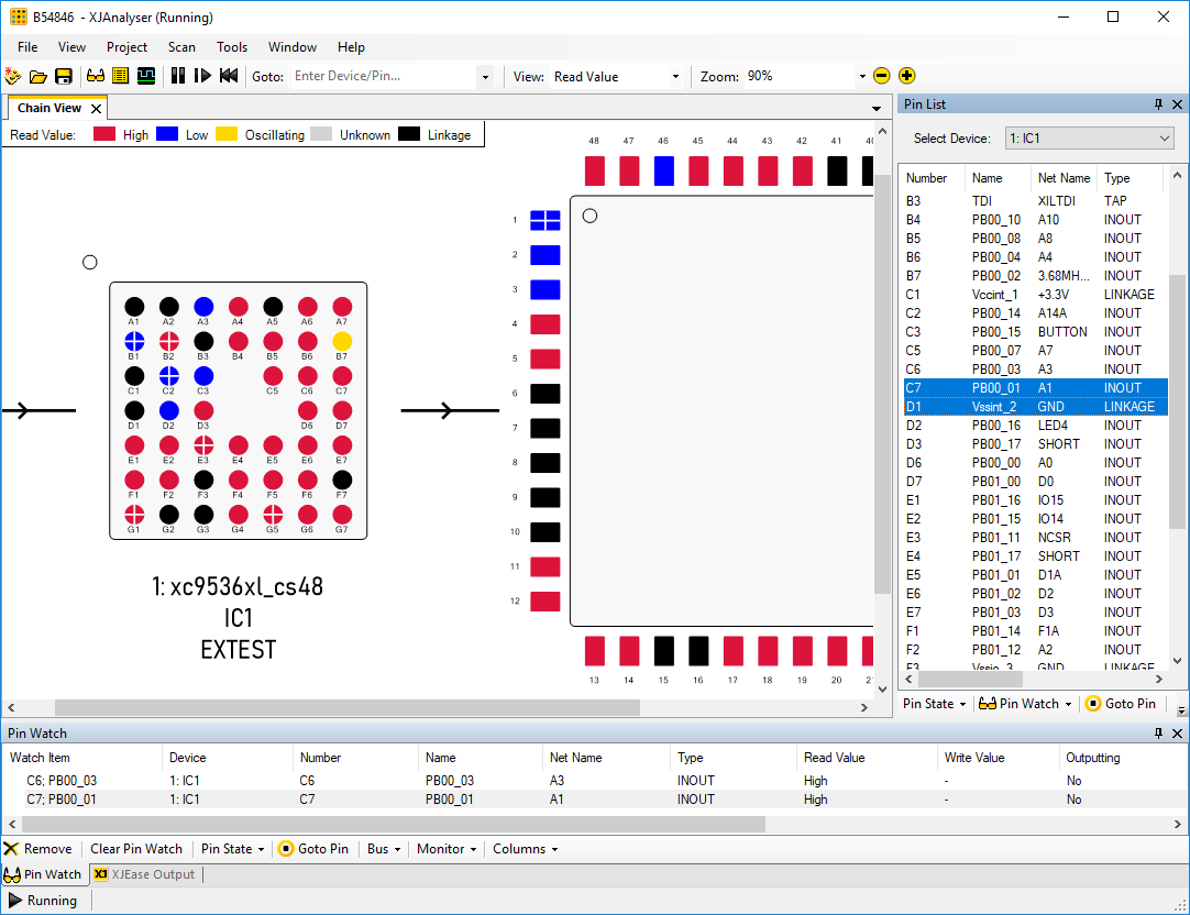
Figure 1 – The main chain window in XJAnalyser
Figure 1 is a screen shot from XJAnalyser showing a JTAG chain consisting of two devices. One of these devices is normally packaged, the other is a BGA device.
The colours of the pins indicate their current values. XJAnalyser can set the values for output and bi-directional pins to high, low, fast oscillating and slow oscillating.
As seen in Figure 1, XJAnalyser can also display information about the pins in a circuit on a per-device basis (the pin list in the right hand pane) or about a selection of pins (the pin watch in the bottom pane). This enables direct access to specific information of interest.
Manufacturing validation
With the integrity of the JTAG chain verified, it is possible to carry out more general tests on the circuit, checking for manufacturing faults.
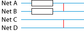
Figure 2 – Short circuit examples
XJTAG’s Connection Test identifies manufacturing faults in three categories: short circuits, open circuits and stuck at faults. Its proprietary Automatic Test Pattern Generation (ATPG) algorithm has been designed to achieve a high percentage of circuit coverage and fault reporting that identifies the exact nature and location of faults.
Figure 2 shows an example of a situation that causes a major problem for many JTAG interconnection tests. While a simple short circuit, such as that shown between nets C and D, can be identified, the inline resistors in nets A and B mean that the short circuit between those two nets may not be detected. XJTAG’s interconnection test algorithm overcomes this problem.
Fault reporting is improved by XJTAG’s ability to react to the current state of the circuit under test. When an inconsistency is identified by the ATPG test, more tests are automatically generated to pinpoint the nature and location of that fault.
Functional testing of non-JTAG devices
Even the most effective interconnection test will not be able to test all of the connections in a circuit. The manner in which XJTAG’s test patterns are generated enables functional testing of a wide range of non-JTAG devices, extending the ability of JTAG to test areas of the circuit away from the JTAG chain.
Figure 3 shows a representation of an XJTAG test system. Here, the XJTAG Runtime Engine reads the ‘XJEase device files, which give it general purpose information on how to test the devices, and then uses information specified in the XJTAG Project File, such as the netlist, to create the relevant test patterns for this specific circuit.
The XJEase device files contain information about the devices and how to test them, but do not contain any information about this particular circuit. This makes the tests re-usable both within and across projects.
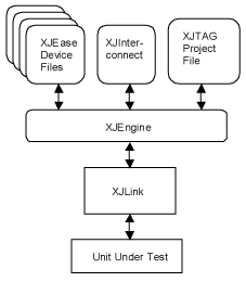
Figure 3 – XJTAG Test Project/System structure
These test patterns are generated as the test system is running, with the current status of devices in the circuit known by the active test, which can use that to programmatically control the next test vector that is generated.
The introduction of programmatic control and reactive test pattern generation to JTAG testing expands both the percentage of a circuit and the range of devices that can be tested. Consider a device that needs to be put into a particular mode to enable testing. With an XJTAG test system, the XJEase device test simply describes the pins that need to be driven for the device to enter the testable mode; the test then loops, reading the device state, until a value is read that indicates that the mode has been entered and the test can proceed. Tests for such a device are only made possible by XJTAG’s circuit interaction.
The multiple levels of abstraction in XJTAG mean that test systems can be developed very quickly.
The abstraction of device testing from circuit implementation, the core of XJTAG’s device-centric philosophy, provides two significant benefits. Firstly, the process of test development is much easier: tests are created by simply describing the pins that need to be set and the values that should result. Secondly, all tests that are developed can be reused whenever that device is used in other circuits and any changes to a circuits netlist will require no reworking of the test system.