High Speed Programming of Everspin Technologies’ PERSYST xSPI MRAM using XJFlash
Introduction
The XJTAG Development System consists of a range of hardware and software tools designed for debugging, testing, and programming electronic circuits, supporting devices that conform to IEEE 1149.1 and 1149.6 JTAG standards.
JTAG was originally conceived for testing the interconnectivity of components on printed circuit boards (PCBs) but has generally been more commonly known for programming and processor debug. More recently, with increasing device complexity and the rise of ball grid array (BGA) and chip scale package (CSP) devices, it has gained importance and popularity in testing due to the ease of access it offers to otherwise hidden pins. However, it is still frequently used for programming non-volatile memories (NVMs).
The traditional method of using JTAG to program NVMs can be slow, prompting the development of faster, more creative programming methods such as XJFlash. This has been sufficient to hit the theoretical maximum programming speed for many years as the limiting factor has been the speed of the NVM device itself, however recent developments with Magnetoresistive Random Access Memory (MRAM) have removed this bottleneck, allowing XJFlash to show its full programming capabilities. This paper outlines the various JTAG-based programming techniques within the XJTAG system and compares their performance.
The JTAG Standard – a brief summary
The JTAG standard uses a cell or cells between a device’s external pin and internal logic to set and retrieve values without direct physical access. These cells can either pass signals directly through from the internal logic, allowing the device to operate as normal, or can disconnect the internal logic and read from or write to the pins directly.
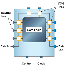
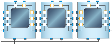
To control these JTAG cells, the JTAG enabled device requires four dedicated pins: TDI (Data In), TDO (Data Out), TMS (Control), and TCK (Clock). Data is shifted serially around the JTAG chain, allowing data to be written in and read out from the cells. If there are multiple JTAG devices on a board, they can be linked together in a chain with TDO from one device connecting to TDI on the next and sharing control and clock signals. This setup allows for control of multiple JTAG devices with a single set of JTAG Test Access Port (TAP) connections.
Traditional JTAG NVM Programming
In traditional JTAG programming from most vendors, the address, data, and control lines of an NVM are set by shifting serial data through the JTAG chain. Using this method, fully programming a flash device via an FPGA involves scanning the full chain twice for every address in the memory. At a typical maximum TCK frequency of 20 MHz, this would mean that a 16-bit, 128 Mbit parallel flash would take a minimum of 7 minutes to program, and SPI flash would take even longer, making it impractical in production environments.
FPGA-Based Flash Programming
FPGAs commonly have direct access to NVMs in the circuit and their JTAG interfaces can be leveraged to speed up programming. It is generally possible to configure the FPGA to handle the programming, allowing the data for the NVM to be copied directly into it and then written to the memory at a much higher speed. In real world environments, we have seen total programming time of the same 16-bit, 128 Mb flash chip brought down to under half a minute, consisting of 5 seconds of overhead to configure the FPGA, followed by around 15 seconds to program the data into the NVM. This method offers significant time savings, making it suitable for development and production. Since the overhead is fixed, the data rate will increase proportionally for larger flash chips. With this method, the limiting factor for programming speed ends up being how fast the flash memory device can be written to, which means we can confidently say that we are programming the device at the maximum possible speed.
What is Everspin Technologies MRAM?
MRAM leverages magnetic states rather than electrical charges to store data, allowing to produce a NVM chip that runs at speeds normally associated with RAM devices, thereby combining the persistent storage of flash memory with the speed and resilience of RAM. This also eliminates the need for backup power sources such as batteries or capacitors, making MRAM particularly well-suited for devices that must function reliably in critical environments. MRAM’s standard interfaces, both parallel and serial, allow for seamless integration, offering low-latency storage and retrieval.
Everspin has recently introduced a new xSPI PERSYST MRAM product family, based on the EXpanded Serial Peripheral Interface, the latest JEDEC standard for non-volatile memory devices. It is based on Everspin’s unique industrial STT-MRAM technology. The products offer high-performance, multiple I/O, SPI-compatibility and feature a high-speed, low pin count SPI compatible bus interface with a clock frequency of up to 200 MHz. These persistent memory MRAM devices operate on a single 1.8 V power supply and deliver up to 400 MBps for both reads and writes via eight I/O signals. This ushers in a new era of universal memory application solutions, replacing products such as SRAM, BBSRAM, NVSRAM and NOR devices, targeting Industrial Automation, Process Control, Emulation, Automotive and Transportation, Gaming, and the broader industrial IoT markets.
Programming Everspin Technologies MRAM devices
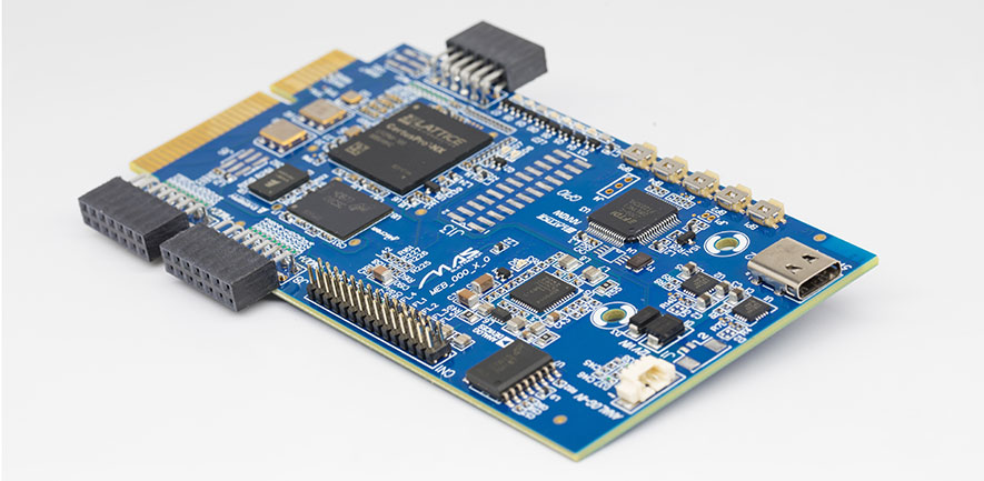
The NVM programming speed limitation changed with the Everspin’s PERSYST xSPI STT-MRAM devices, such as EM064LXO and EM128LXO, with octal xSPI interfaces. We have been testing using XJFlash to write to one of these chips, on a board provided by MAS Elettronica (the MAS Educational Board, pictured below), and now that the write speed is no longer limited by the storage medium, we have achieved sustained data transfer rates of 32 Mbit/s, allowing us to initialise and program an 8 megabyte MRAM device with pseudorandom data in around 2 seconds. As XJFlash uses data compression to increase the transfer rate over the JTAG link, this speed would be even faster with real world data, however the 32 Mbit/s provides a tested minimum speed.
Since the write speed of the NVM is no longer the limiting factor, XJFlash can program the device as fast as data can be sent over the JTAG link. In this case, that was limited by the FPGA’s maximum supported TCK speed of 55 MHz, however as technology continues to improve, we expect this to increase further.
Currently, XJTAG’s full range of controllers, the XJLink2 and XJLink-PF40, support TCK speeds up to 166 MHz, which means there’s still room for the data transfer speed to be increased even further, potentially over 100 Mb/s, by using FPGAs and circuits that support faster TCK speeds. Everspin’s top of the line MRAM devices currently support write speeds of 400 MB/s, so there’s plenty of room for growth. The programming currently only takes a few seconds at 32 Mb/s, so whilst any future speed improvements would just make this even better, it’s already easily fast enough to be incorporated into the normal circuit testing process without increasing cycle time of testing stations on the production line.
With Everspin’s MRAM devices, in-situ programming is even more important as the persistent storage is sensitive to heat – the device state cannot be guaranteed after a solder reflow operation, hence a full device initialization and configuration is required. It would be possible to add additional data lines to the board, allowing the MRAM to be programmed by an external connection, however this would add design complexity and likely degrade real world performance due to longer data traces picking up noise, so given how fast JTAG programming can be with XJFlash, programming as part of the test process makes the most sense.
Conclusion
XJTAG has been making high speed programming of flash devices possible for many years, increasing programming speeds by an order of magnitude compared to traditional JTAG programming, and so making programming through a JTAG connection a competitive proposition. Flash devices of a size which would take several minutes to program traditionally can be programmed in 15-20 seconds using XJFlash acceleration. Now, with the release of Everspin Technologies PERSYST xSPI MRAM devices, programming speed can be increased by an additional order of magnitude, bringing MRAM device programming times down to just a few seconds. The effect of this is that programming of larger NVMs can now be integrated into the production line as part of the testing process, without fear of holding up the line.
For more information, please contact us.