Layout Viewer
Overview
Layout Viewer provides the capability to view layout design data extracted from ODB++ files, including highlighting different layers of the board, individual components and individual nets. Powerful search functionality allows you to quickly find the physical location of components, nets and pins on a board through a simple interface.
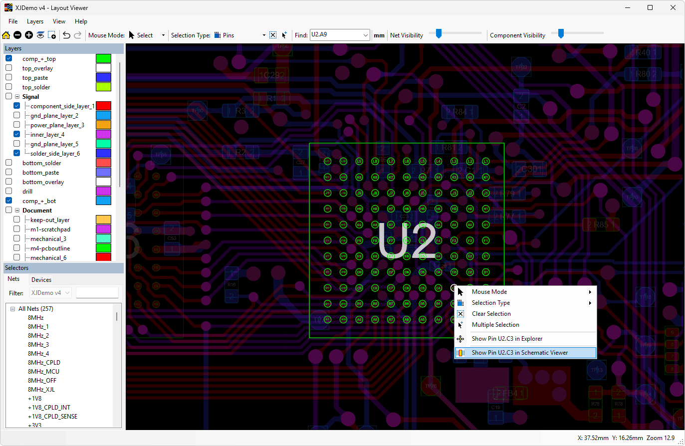
XJBoardExplorer offers all this plus direct integration with the schematic viewer, allowing any pin, device or net to be selected in one and displayed in the other. Additionally, device information can be displayed separately, showing BOM information, busses and pin details.
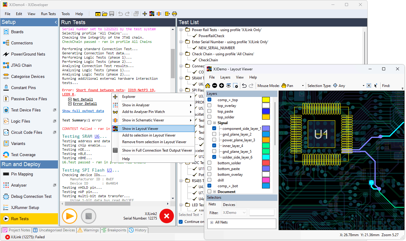
If you’re using applications of XJTAG’s Test Suite such as XJDeveloper, XJInvestigator and XJRunner, you can use the Layout Viewer to visualise any faults that are found when running tests. The Connection Test output includes clickable links to directly display all of the relevant circuit elements. XJEase tests can also output links to display devices, pins and nets in the circuit layout.
Key Benefit
- Improve productivity by visualising the exact location of items on the PCB or faults to be repaired
Features
- Aids identifying likely points of failure.
- Measures distance between objects.
- Control over which layers are visible.
- Advanced layer and zoom controls.
- Exports graphics to the clipboard, a file or printer.
- Import board pictures for clearer display
Included with XJBoardExplorer and XJDeveloper/XJInvestigator/XJRunner systems
Layout Viewer is integrated into XJBoardExplorer for fast and easy exploration of your circuit design.
It is also integrated into XJDeveloper, XJInvestigator and XJRunner tests to help engineers quickly identify faults on a connected board.
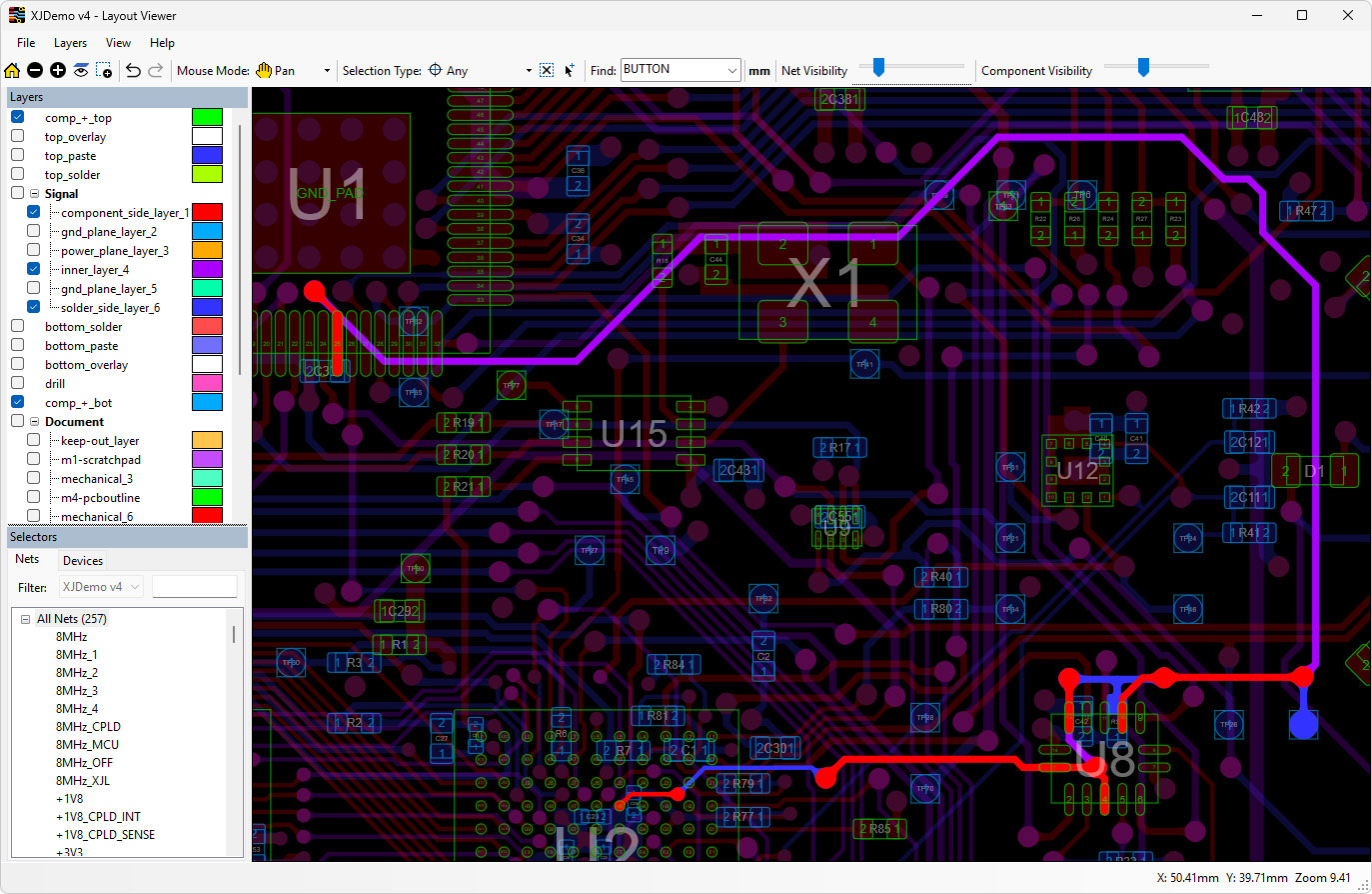
Visualise circuit elements
The advanced graphical display highlights selected components and nets. Individual layers can be turned on or off as required to make it easy to see specific circuit elements.
Determine the location of faults within seconds
The Layout Viewer can be used to quickly locate where faults are on the board under test.
When used with XJRunner or XJInvestigator, the test output provides details about the types of fault and which nets are involved, with clickable links to easily display the fault in the Layout Viewer. By showing the routing of nets, the Layout Viewer helps to locate the fault on the physical board by showing the potential problem areas.
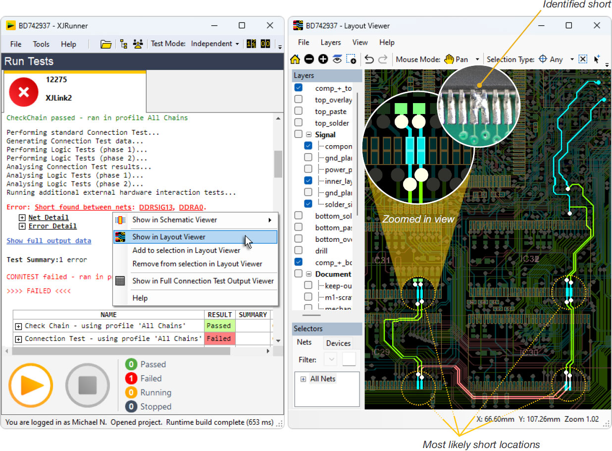
In this particular example, XJRunner reports that the Connection Test has failed, and has identified two nets that are shorted together. By looking at the layout, it is easy to determine that the four most likely locations are the pads on the memory devices. It is unlikely that the fault is under the BGA device as the pins are not next to each other.
By examining the four locations on the board, it was quickly identified that the problem was a soldering fault on IC31.
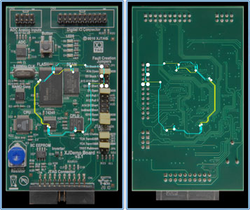
Import board pictures
For even more help in identifying where on a board the faults are located, pictures of the front and the back of the board can be imported. These images can then be displayed behind the CAD data with its highlighted components and nets.
Supported features
| XJBoardExplorer | XJDeveloper & XJRunner | |
| Import ODB++ files | ✓ | ✓ |
| Display board layout | ✓ | ✓ |
| Search for components, pins or nets | ✓ | ✓ |
| Highlight any net, component and pin | ✓ | ✓ |
| Jump from layout to schematic view with one click | ✓ | ✓ |
| Integration with board tests | ✓ | |
| Displays UUT fault information | ✓ |